asokatechnologies@gmail.com 09347143789/09949240245

Search This Blog

Friday, 14 November 2014

A ZVS Grid-Connected Three-Phase Inverter

A ZVS Grid-Connected Three-Phase Inverter

ABSTRACT:

A six-switch three-phase inverter is widely used in a high-power grid-connected system. However, the anti parallel diodes in the topology operate in the hard-switching state under the traditional control method causing severe switch loss and high electromagnetic interference problems. In order to solve the problem, this paper proposes a topology of the traditional six-switch three-phase inverter but with an additional switch and gave a new space vector modulation (SVM) scheme. In this way, the inverter can realize zero-voltage switching (ZVS) operation in all switching devices and suppress the reverse recovery current in all anti parallel diodes very well. And all the switches can operate at a fixed frequency with the new SVM scheme and have the same voltage stress as the dc-link voltage. In grid-connected application, the inverter can achieve ZVS in all the switches under the load with unity power factor or less. The aforementioned theory is verified in a 30-kW inverter prototype.

KEYWORDS:

1.      Grid connected
2.       soft switching
3.       space vector modulation (SVM)
4.       three-phase inverter
5.       zero-voltage switching (ZVS)

SOFTWARE: MATLAB/SIMULINK

BLOCK DIAGRAM:


Fig. 1.Soft-switching three-phase inverter topology: (a) dc-side topology and (b) ac-side topology.


CONCLUSION:

The analysis and experimentation presented verify that the SVM-controlled three-phase soft-switching grid-connected inverter can realize ZVS operation for all switching devices, and the reverse recovery current in the antiparallel diodes of all switching devices is suppressed well. SVM can be realized at the fixed switching frequency. And the switching voltage stress across all the power switch devices is the same as the dc-link voltage. The ZVS can be achieved in the grid-connected ZVS inverters under the load with unity power factor or less. The reduced switching loss increases its efficiency and makes it suitable for practical applications.

REFERENCES:

[1] N. Mohan, T. Undeland, andW. Robbins, Power Electronics: Converters, Applications and Design. New York: Wiley, 2003, pp. 524–545.
[2] M. D. Bellar, T. S. Wu, A. Tchamdjou, J. Mahdavi, and M. Ehsani, “A review of soft-switched DC–AC converters,” IEEE Trans. Ind. Appl., vol. 34, no. 4, pp. 847–860, Jul./Aug. 1998.
[3] D. M. Divan, “Static power conversion method and apparatus having essentially zero switching losses and clamped voltage levels,” U.S. Patent 48 64 483, Sep. 5, 1989.
[4] M. Nakaok, H. Yonemori, and K. Yurugi, “Zero-voltage soft-switched PDM three phase AC–DC active power converter operating at unity power factor and sinewave line current,” in Proc. IEEE Power Electronics Spec. Conf., 1993, pp. 787–794.

[5] H. Yonemori, H. Fukuda, and M. Nakaoka, “Advanced three-phase ZVSPWM active power rectifier with new resonant DC link and its digital control scheme,” in Proc. IEE Power Electron. Variable Speed Drives, 1994, pp. 608–613.

Research on Three-phase Voltage Type PWM Rectifier System Based on SVPWM Control

Research on Three-phase Voltage Type PWM Rectifier System Based on SVPWM Control


ABSTRACT:

The fundamental principle of SVPWM is introduced in this study. The design on the structure of three phase voltage type PWM rectifier system based on SVPWM control was also discussed. Then we calculate the DC capacitor and AC side inductance. The computer simulation tool MATLAB/Simulink is taken and the result is shown in the end. The result indicates that the design of such platform is feasible.

KEYWORDS:

1.      Power factor
2.       PWM rectifier
3.       space voltage vector
4.       three-phase voltage


SOFTWARE: MATLAB/SIMULINK

 BLOCK DIAGRAM:


Fig. 1: The three phase PWM rectifier voltage fixed vector control diagram


CONCLUSION:

This study introduces SVPWM control principles and adopts three-phase PWM rectifier digital control system based on SVPWM control on the basis of this. Besides, AC-side incoming inductance and DC-side capacitance are calculated and selected. Then, each simulation module is established for the whole system by use of simulation software MATLAB/Simulink and simulation researches are conducted. The simulation result shows the digital control system designed is feasible.

REFERENCES:


 Boon, T.O. and W. Xiao, 1990. Voltage angle lock loop control of the boost type PWM converter for HVDC application [J]. IEEE Tran. Power Elec., 5(2): 229-235.
Fujita, H., Y. Watanabe and H. Akayi, 1998. Control and ana1ysis of a unified power flow controller [J]. IEEE PELS, 98: 805-811.
Li, Z., J. Wang and L. Huade, 2006. Review on nonlinear control strategies of three phase boosttype PWM rectifiers. Electric Drive, 36(1): 9-13.
Marian, P.K. and M. Luigi, 1998. Current control techniques for three-phase voltage-source PWM converters [J]. A survey. IEEE Trans. Power Elec., 45(5): 508-515.

Mariusz, M., M. Jasin’ski and P.K. Marian, 2004. Simple direct power control of three-phase PWM  rectifier using space-vector modulation [J]. IEEE Trans. Ind. Elec., 51(2): 447-454.

Simulation Analysis of SVPWM Inverter Fed Induction Motor Drives

Simulation Analysis of SVPWM Inverter Fed Induction Motor Drives

ABSTRACT:

In this paper represent the simulation analysis of space vector pulse width modulated(SVPWM) inverter fed Induction motor drives. The main objective of this paper is analysis of Induction motor with SVPWM fed inverter and harmonic analysis of voltages & current. for control of IM number of Pulse width modulation (PWM) schemes are used to for variable voltage and frequency supply. The most commonly used PWM schemes for three-phase voltage source inverters (VSI) are sinusoidal PWM (SPWM) and space vector PWM (SVPWM). There is an increasing trend of using space vector PWM (SVPWM) because of it reduces harmonic content in voltage, Increase fundamental output voltage by 15% & smooth control of IM. So, here present Modeling & Simulation of SVPWM inverter fed Induction motor drive in MATLAB/SIMULINK software. The results of Total Harmonic Distortion (THD), Fast Fourier Transform (FFT) of current are obtained in MATLAB/Simulink software.

KEYWORDS:
1.      Inverter
2.       VSI
3.       SPWM
4.       SVPWM
5.       IM drive


SOFTWARE: MATLAB/SIMULINK

BLOCK DIAGRAM:


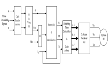
Figure 1 Simulation Block Diag. of SVPWM Three level inverter with IM load


CONCLUSION:

The SVPWM Inverter fed induction motor drive Modeling & then simulation is done in MATLAB/SIMULINK 12. From simulation results of THD & FFT analysis concluded that SVPWM technique is better over all PWM techniques which gives less THD in Inverter current 4.89%., which under the permissible limit.


REFERENCES:

 [1] A. R. Bakhshai H. R. Saligheh Rad G. Joos, space vector modulation based on classification method in three-phase multi-level voltage source inverters, IEEE 2001
[2] Bimal K Bose, modern power electronics and ac drives © 2002 Prentice hall ptr.
[3] Dorin O. Neacsu, space vector modulation –An introduction tutorial at IECON2001 IEEE 2001
[4] Fei Wang, Senior Member, “Sine-Triangle versus Space-Vector Modulation for Three-Level PWM Voltage-Source Inverters”, IEEE transactions on industry applications, vol. 38, no. 2, March/April 2002. The 27th Annual Conference of the IEEE Industrial Electronics Society

[5] F. Wang, Senior, Sine-Triangle vs. space vector modulation for three-level voltage source inverters ,IEEE 2000

A High-Efficiency Wide-Input-Voltage Range Switched Capacitor Point-of-Load DC–DC Converter

A High-Efficiency Wide-Input-Voltage Range Switched Capacitor Point-of-Load DC–DC Converter

ABSTRACT:

The traditional inductor-based buck converter has been the default design for switched-mode voltage regulators for decades. Switched capacitor (SC) dc–dc converters, on the other hand, have traditionally been used in low-power (<10 mW) and low conversion ratio (<4:1) applications where neither regulation nor efficiency is critical. This study encompasses the complete successful design, fabrication, and test of a CMOS-based SC dc–dc converter, addressing the ubiquitous 12–1.5 V board mounted point-of-load application. In particular, the circuit developed in this study attains higher efficiency (92% peak, and >80% over a load range of 5 mA to 1 A) than surveyed competitive buck converters, while requiring less board area and less costly passive components. The topology and controller enable a wide input range of 7.5–13.5 V. Controls based on feedback and feed forward provide tight regulation under worst case line and load step conditions. This study shows that the SC converter can outperform the buck
 converter, and thus, the scope of SC converter application can and should be expanded.

KEYWORDS:

1.      DC-DC power converters
2.       switched capacitor circuits
3.      switched-mode power supply

SOFTWARE: MATLAB/SIMULINK

BLOCK DIAGRAM:


 Fig. 1. Overall block diagram of the controller.

CONCLUSION:

The traditional inductor-based buck converter has been the default design for switched-mode voltage regulators for decades. Switched capacitor (SC) dc–dc converters, on the other hand, have traditionally been used in low-power (<10 mW) and low conversion ratio (<4:1) applications where neither regulation nor efficiency is critical. This study encompasses the complete successful design, fabrication, and test of a CMOS-based SC dc–dc converter, addressing the ubiquitous 12–1.5 V board mounted point-of-load application. In particular, the circuit developed in this study attains higher efficiency (92% peak, and >80% over a load range of 5 mA to 1 A) than surveyed competitive buck converters, while requiring less board area and less costly passive components. The topology and controller enable a wide input range of 7.5–13.5 V. Controls based on feedback and feed forward provide tight regulation under worst case line and load step conditions. This study shows that the SC converter can outperform the buck converter, and thus, the scope of SC converter application can and should be expanded.

REFERENCES:

[1] M. Seeman and S. Sanders, “Analysis and optimization of switched capacitor dc–dc converters,” IEEE Trans. Power Electron., vol. 23, no. 2, pp. 841–851, Mar. 2008.
[2] M. Seeman,V.Ng, H.-P. Le,M. John, E. Aton, and S. Sanders, “Acomparative analysis of switched-capacitor and inductor-based dc–dc conversion technologies,” in Proc. IEEE Workshop Control Model. Power Electron. (COMPEL), Jun. 2010.
[3] M. Seeman, “A design methodology for switched-capacitor dc-dc converters,” Ph.D. dissertation, UC Berkeley, Berkeley, CA, May 2009.
[4] High Efficiency, 250 mA Step-Down Charge Pump, Texas Instruments (TPS60503), Dallas, TX, 2002.
[5] 500 mA High Efficiency, Low Noise, Inductor-Less Step-Down DC/DC Converter, Linear Technology (LTC3251), Milpitas, CA, 2003.

Wednesday, 12 November 2014

Fuzzy-Logic-Controller-Based SEPIC Converter for Maximum Power Point Tracking

Fuzzy-Logic-Controller-Based SEPIC Converter for
Maximum Power Point Tracking

ABSTRACT:

This paper presents a fuzzy logic controller (FLC)-based single-ended primary-inductor converter (SEPIC) for maximum power point tracking (MPPT) operation of a photovoltaic (PV) system. The FLC proposed presents that the convergent distribution of the membership function offers faster response than the symmetrically distributed membership functions. The fuzzy controller for the SEPIC MPPT scheme shows high precision in current transition and keeps the voltage without any changes, in the variable-load case, represented in small steady-state error and small overshoot. The proposed scheme ensures optimal use of PV array and proves its efficacy in variable load conditions, unity, and lagging power factor at the inverter output (load) side. The real-time implementation of the MPPT SEPIC converter is done by a digital signal processor (DSP), i.e., TMS320F28335. The performance of the converter is tested in both simulation and experiment at different operating conditions. The performance of the proposed FLC-based MPPT operation of SEPIC converter is compared to that of the conventional proportional–integral (PI)-based SEPIC converter. The results show that the proposed FLC-based MPPT scheme for SEPIC can accurately track the reference signal and transfer power around 4.8% more than the conventional PI-based system.

KEYWORDS:
1.     DC–DC power converters
2.     Fuzzy control
3.     Photovoltaic(PV) cells
4.     Proportional–integral (PI) controller
5.     Real-time system.


SOFTWARE: MATLAB/SIMULINK

BLOCK DIAGRAM:


          Fig. 1. Overall control scheme for the proposed FLC-based MPPT scheme for the SEPIC converter.


CONCLUSION:

An FLC-based MPPT scheme for the SEPIC converter and inverter system for PV power applications has been presented in this paper. A prototype SEPIC converter-based PV inverter system has also been built in the laboratory. The DSP board TMS320F28335 is used for real-time implementation of the proposed FLC and MPPT control algorithms. The performance of the proposed controller has been found better than that of the conventional PI-based converters. Furthermore, as compared to the conventional multilevel inverter, experimental results indicated that the proposed FLC scheme can provide a better THD level at the inverter output. Thus, it reduces the cost of the inverter and the associated complexity in control algorithms. Therefore, the proposed FLC-based MPPT scheme for the SEPIC converter could be a potential candidate for real-time PV inverter applications under variable load conditions.

REFERENCES:

[1] K.M. Tsang andW. L. Chan, “Fast acting regenerative DC electronic load based on a SEPIC converter,” IEEE Trans. Power Electron., vol. 27, no. 1, pp. 269–275, Jan. 2012.
[2] S. J. Chiang, H.-J. Shieh, and M.-C. Chen, “Modeling and control of PV charger system with SEPIC converter,” IEEE Trans. Ind. Electron., vol. 56, no. 11, pp. 4344–4353, Nov. 2009.
[3] M. G. Umamaheswari, G. Uma, and K. M. Vijayalakshmi, “Design and implementation of reduced-order sliding mode controller for higher-order power factor correction converters,” IET Power Electron., vol. 4, no. 9, pp. 984–992, Nov. 2011.
[4] A. A. Fardoun, E. H. Ismail, A. J. Sabzali, and M. A. Al-Saffar, “New efficient bridgeless Cuk rectifiers for PFC applications,” IEEE Trans. Power Electron., vol. 27, no. 7, pp. 3292–3301, Jul. 2012.


Friday, 7 November 2014

A Novel Three-Phase Three-Leg AC/AC Converter Using Nine IGBTs

A Novel Three-Phase Three-Leg AC/AC Converter Using Nine IGBTs

ABSTRACT:
This paper proposes a novel three-phase nine-switch ac/ac converter topology. This converter features sinusoidal inputs and outputs, unity input power factor, and more importantly, low manufacturing cost due to its reduced number of active switches. The operating principle of the converter is elaborated; its modulation schemes are discussed. Simulated semiconductor loss analysis and comparison with the back-to-back two-level voltage source converter are presented. Finally, experimental results from a 5-kVA prototype system are provided to verify the validity of the proposed topology.

KEYWORDS:

1.      AC/AC converter
2.       pulse width modulation (PWM)
3.      reduced switch count topology


SOFTWARE: MATLAB/SIMULINK


CIRCUIT DIAGRAM:


                                                        Fig: 1 B2B 2L-VSC.


 CONCLUSION:
A novel nine-switch PWMac/ac converter topology was proposed in this paper. The topology uses only nine IGBT devices for ac to ac conversion through a quasi dc-link circuit. Compared with the conventional back-to-back PWM VSC using 12 switches and the matrix converter that uses 18, the number of switches in the proposed converter is reduced by 33% and 50%, respectively. The proposed converter features sinusoidal inputs and outputs, unity input power factor, and low manufacturing cost. The operating principle of the converter was elaborated, and modulation schemes for constant and VF operations were developed. Simulation results including a semiconductor loss analysis and comparison were provided, which reveal that the proposed converter, while working in CF mode, has an overall higher efficiency than the B2B 2L-VSC at the expense of uneven loss distribution. However, the VF-mode version requires IGBT devices with higher ratings and dissipates significantly higher losses, and thus, is not as attractive as its counterpart. Experimental verification is carried out on a 5-kVA prototype system.

REFERENCES:

[1] B. Wu, High-power Converters and AC Drives. Piscataway, NJ: IEEE/Wiley, 2006.
[2] B. Singh, B. N. Singh, A. Chandra, K. Al-Haddad, A. Pandey, and D. P. Kothari, “A review of three-phase improved power quality AC– DC converters,” IEEE Trans. Ind. Electron., vol. 51, no. 3, pp. 641–660, Jun. 2004.
[3] F. Blaabjerg, S. Freysson, H. H. Hansen, and S. Hansen, “A new optimized space-vector modulation strategy for a component-minimized Voltage source inverter,” IEEE Trans. Power Electron., vol. 12, no. 4, pp. 704–714, Jul. 1997.

[4] R. L. A. Ribeiro, C. B. Jacobina, E. R. C. da Silva, and A. M. N. Lima, “AC/AC converter with four switch three phase structures,” in Proc. IEEE PESC, 1996, vol. 1, pp. 134–139.

Tuesday, 4 November 2014

A Novel Zero-Voltage-Switching PWM Full Bridge Converter

A Novel Zero-Voltage-Switching PWM Full Bridge Converter


ABSTRACT

Introducing resonant inductance and clamping diodes into the full-bridge converter can eliminate the voltage oscillation across the rectifier diodes and increase the load range for zero-voltage-switching (ZVS) achievement. The resonant inductance is shorted and its current keeps constant when the clamping diode is conducting, and the clamping diode is hard turned-off, causing significant reverse recovery loss if the output filter inductance is relatively larger. This paper improves the full-bridge converter by introducing a reset winding in series with the resonant inductance to make the clamping diode current decay rapidly when it conducts. The reset winding not only reduces the conduction losses, but also makes the clamping diodes naturally turn-off and avoids the reverse recovery. The operation principle of the proposed converter is analyzed. The design of the turns ratio of transformer is discussed. A 1 kW prototype converter is built to verify the operation principle and the experimental results are also demonstrated.

KEYWORDS
      1.  Clamping diodes
        2.    Full bridge converter
        3.    Reset winding
        4.    Zero-voltage-switching (ZVS)

SOFTWARE: MATLAB/SIMULINK


BLOCK DIAGRAM:

Fig.1. Proposed ZVS PWM full bridge converter.(a) Tr_ lag  type. (b) Trlead  type.


CONCLUSION:

A new ZVS PWM full-bridge converter is proposed in this   paper, it employs an additional reset winding to make the clamping diode current decay rapidly when the clamping diode conducts, thus the conduction losses of the clamping diodes, the leading switches and the resonant inductance are reduced and the conversion efficiency can be increased. In the meanwhile, the clamping diodes can be turned off naturally without reverse recovery over the whole input voltage range, and the output filter inductance can be designed to be large to obtain small current ripple, leading to reduced filter capacitance. Compared with the traditional full bridge converter [14]–[16], the proposed circuit provides another simple and effective approach to avoid the reverse recovery of the clamping diodes. The operation principle, features and comparisons are illustrated. The Experimental results from the prototype are shown to verify the feasibility of the proposed converter.

REFERENCES:

[1] X. Ruan and Y. Yan, “Soft-switching techniques for pwm full bridge converters,” in Proc. IEEE Power Electron. Spec. Conf. (PESC’00), 2000, pp. 634–639.
[2] D. M. Sable and F. C. Lee, “The operation of a full-Bridge, zero voltage- switched pwm converter,” in Proc. Virginia Power Electron. Center (VPEC’89), 1989, pp. 92–97.
[3] J. A. Sabate, V. Vlatkovic, R. B. Ridley, F. C. Lee, and B. H. Cho, “Design considerations for high-voltage, high power full-bridge zero voltage- switched pwm converter,” in Proc. IEEE Appl. Power Electron. Conf. (APEC’90), 1990, pp. 275–284.

[4] G. C. Hua, F. C. Lee, and M. M. Jovanovic, “An improved zero-voltage-switched pwm converter using a saturable inductor,” in Proc. IEEE Power Electron. Spec. Conf. (PESC’91), 1991, pp. 189–194.