asokatechnologies@gmail.com 09347143789/09949240245

Search This Blog

Friday 27 April 2018

Versatile Unified Power Quality Conditioner Applied to Three-Phase Four-Wire Distribution Systems Using a Dual Control Strategy


ABSTRACT:

 This paper presents the study, analysis and practical implementation of a versatile unified power quality conditioner (UPQC), which can be connected in both three-phase three-wire or three-phase four-wire distribution systems for performing the series-parallel power-line conditioning. Thus, even when only a three-phase three-wire power system is available at a plant site, the UPQC is able to carry out power-line compensation for installed loads that require a neutral conductor to operate. Different from the control strategies used in the most of UPQC applications in which the controlled quantities are non-sinusoidal, this UPQC employs a dual compensation strategy, such that the controlled quantities are always sinusoidal. Thereby, the series converter is controlled to act as a sinusoidal current source, whereas the parallel converter operates as a sinusoidal voltage source. Thus, because the controlled quantities are sinusoidal, it is possible to reduce the complexity of the algorithms used to calculate the compensation references. Therefore, since the voltage and current controllers are implemented into the synchronous reference frame, their control references are continuous, decreasing the steady-state errors when traditional proportional-integral controllers are employed. Static and dynamic performances, as well as the effectiveness of the dual UPQC are evaluated by means of experimental results.
 KEYWORDS:
1.      Active filter
2.      Dual control strategy
3.       Power conditioning
4.       Three-phase distribution systems
5.       UPQC
SOFTWARE: MATLAB/SIMULINK

CIRCUIT DIAGRAM:


Fig. 1. 3P4W distribution system based on UPQC topology connected to 3P3W power system.


 EXPECTED SIMULATION RESULTS:


 Fig. 2. Experimental results for the loads presented in Table III: (a) UPQC currents for unbalanced three-phase -phase load (1) (20 A/div, 5 ms/div): Load currents (π‘–πΏπ‘Ž, 𝑖𝐿𝑏, 𝑖𝐿𝑐) and 𝑖𝐿𝑛, Compensated source currents (π‘–π‘ π‘Ž, 𝑖𝑠𝑏, 𝑖𝑠𝑐), and Currents of the parallel converter (π‘–π‘π‘Ž, 𝑖𝑐𝑏, 𝑖𝑐𝑐) and 𝑖𝑐𝑛; (b) Currents and voltages of phase “a” of the UPQC for the unbalanced three-phase load (2) (20 A/div, 100V/div, 5 ms/div): Load currents (π‘–πΏπ‘Ž, 𝑖𝐿𝑏, 𝑖𝐿𝑐); Currents of phase “a”: load π‘–πΏπ‘Ž, parallel converter π‘–π‘π‘Ž and source π‘–π‘ π‘Ž; voltages and currents of phase “a”: load current π‘–πΏπ‘Ž , source current π‘–π‘ π‘Ž, utility voltage π‘£π‘ π‘Ž and load voltage π‘£πΏπ‘Ž, (c) UPQC currents for three-phase load (1) (2.5 ms/div): Load currents (π‘–πΏπ‘Ž, 𝑖𝐿𝑏, 𝑖𝐿𝑐) (5 A/div), Source compensated currents (π‘–π‘ π‘Ž, 𝑖𝑠𝑏, 𝑖𝑠𝑐) (10 A/div), Parallel converter currents (π‘–π‘π‘Ž, 𝑖𝑐𝑏, 𝑖𝑐𝑐) (10 A/div).


Fig. 3. Voltages of the UPQC under utility harmonics and unbalances for the unbalanced three-phase load (1): (a) Utility voltages (π‘£π‘ π‘Ž, 𝑣𝑠𝑏, 𝑣𝑠𝑐) (50 V/div, 2,5ms/div), Load voltages (π‘£πΏπ‘Ž, 𝑣𝐿𝑏, 𝑣𝑠𝐿) (50 V/div, 2,5ms/div) and series compensating voltages (π‘£πΆπ‘Ž, 𝑣𝐢𝑏 and 𝑣𝐢𝑐) (50 V/div, 2,5ms/div); (b) (a) Utility voltages (π‘£π‘ π‘Ž, 𝑣𝑠𝑏, 𝑣𝑠𝑐) (50 V/div, 2,5ms/div), Load voltages (π‘£πΏπ‘Ž, 𝑣𝐿𝑏, 𝑣𝑠𝐿) (50 V/div, 2,5ms/div) and series compensating voltages (π‘£πΆπ‘Ž, 𝑣𝐢𝑏 and 𝑣𝐢𝑐) (50 V/div, 2,5ms/div)


Fig. 4. Voltages and current of the UPQC for the unbalanced three-phase load 1: (a) DC-bus voltage (𝑉𝐷𝐢) (100 V/div, 500ms/div) and load currents (π‘–πΏπ‘Ž, 𝑖𝐿𝑏, 𝑖𝐿𝑐) (20 A/div, 500ms/div); (b) DC-bus voltage (𝑉𝐷𝐢) (100 V/div, 500ms/div) and source currents (π‘–π‘ π‘Ž, 𝑖𝑠𝑏, 𝑖𝑠𝑐) (20 A/div, 500ms/div); (c) DC-bus voltage (𝑉𝐷𝐢) (100 V/div, 5ms/div) and details of the source currents (π‘–π‘ π‘Ž, 𝑖𝑠��, 𝑖𝑠𝑐) after the first load transient (20 A/div, 5ms/div).


Fig. 5. UPQC under voltage sag disturbance (phase ‘a’): utility voltage (π‘£π‘ π‘Ž), load voltage (π‘£πΏπ‘Ž) and series compensating voltage (π‘£πΆπ‘Ž) (200 V/div, 25ms/div).


CONCLUSION:
This paper presents a practical and versatile application based on UPQC, which can be used in three-phase three-wire (3P3W), as well as three-phase four-wire (3P4W) distribution systems. It was demonstrated that the UPQC installed at a 3P3W system plant site was able to perform universal active filtering even when the installed loads required a neutral conductor for connecting one or more single-phase loads (3P4W). The series-parallel active filtering allowed balanced and sinusoidal input currents, as well as balanced, sinusoidal and regulated output voltages. By using a dual control compensating strategy, the controlled voltage and current quantities are always sinusoidal. Therefore, it is possible to reduce the complexity of the algorithms used to calculate the compensation references. Furthermore, since voltage and current SRF-based controllers are employed, the control references become continuous, reducing the steady-state errors when conventional PI controllers are used. Based on digital signal processing and by means of extensive experimental tests, static and dynamic performances, as well as the effectiveness of the dual UPQC were evaluated, validating the theoretical development.
REFERENCES:

[1] H. Fujita, and H. Akagi, “The unified power quality conditioner: The integration of series and shunt active filters,” IEEE Trans. Power Electron., vol. 13, no. 2, pp. 315-322, Mar. 1998.
[2] R. J. M. Santos,. J. C. Cunha, and M. Mezaroba, “A simplified control technique for a dual unified power quality conditioner,” IEEE Trans. Ind. Electron., vol. 61, no. 11, pp. 5851-5860, Nov. 2014.
[3] B.W. FranΓ§a, L.F. Silva, M. A Aredes, and M., Aredes, “An improved iUPQC controller to provide additional grid-voltage regulation as a STATCOM,” IEEE Trans. Ind. Electron., , vol. 62, no. 3, pp. 1345-1352, Mar. 2015.
[4] R. A. Modesto, S. A. O. Silva, and A. A., Oliveira, “Power quality improvement using a dual unified power quality conditioner/uninterruptible power supply in three-phase four-wire systems,” IET Power Electronics, vol. 8, no. 3, pp. 1595-1605, Sept. 2015.
[5] V. Khadkikar, “Enhancing electric power quality using UPQC: A comprehensive overview,” IEEE Trans. Power Electron., vol. 27, no. 5, pp. 2284-2297, May 2012.


A Novel Five-Level Voltage Source Inverter With Sinusoidal Pulse Width Modulator for Medium-Voltage Applications


 ABSTRACT:
This paper proposes a new five-level voltage source inverter for medium-voltage high-power applications. The proposed inverter is based on the upgrade of a four-level nested neutral-point clamped converter. This inverter can operate over a wide range of voltages without the need for connecting power semiconductor in series, has high-quality output voltage and fewer components compared to other classic five-level topologies. The features and operation of the proposed converter are studied and a simple sinusoidal PWM scheme is developed to control and balance the flying capacitors to their desired values. The performance of the proposed converter is evaluated by simulation and experimental results.

KEYWORDS:
1.      Multilevel converter
2.      Dc–ac power conversion
3.      Sinusoidal pulse width modulation (SPWM)

 SOFTWARE: MATLAB/SIMULINK

 CIRCUIT DIAGRAM:


Fig. 1. New five-level three-phase inverter.

EXPECTED SIMULATION RESULTS:


Fig. 2. Simulation waveforms in steady-state condition (a) inverter voltage, (b) output currents, and (c) voltages of flying capacitors (m = 0.95).

Fig. 3. Simulation waveforms in steady-state condition (a) inverter voltage,
(b) output currents, and (c) voltages of flying capacitors (m = 0.65).

Fig. 4. Simulation waveforms in steady-state condition (inductive load) (a)
inverter voltage, (b) output currents, and (c) voltages of flying capacitors (m =
0.95, PF = 0.7).

Fig. 5. Simulation waveforms in steady-state condition (capacitive load)
(a) inverter voltage, (b) output currents, and (c) voltages of flying capacitors
(m = 0.9, PF = 0.7).

Fig. 6. Simulation waveforms in transient-state condition; load changes from
half-load to full-load (a) inverter voltage, (b) output currents, and (c) voltages
of flying capacitors (m = 0.95).


Fig. 7. Simulation waveforms; voltage of flying capacitors with and without
the controller

CONCLUSION:
This paper introduces a new five-level voltage source inverter for medium-voltage applications. The proposed topology is the upgrade of the four-level NNPC converter that can operate over a wide range of input voltage without any power semiconductor in series. The proposed converter has fewer components as com- pared with classic multilevel converters and the voltage across the power semiconductors is only one-fourth of the dc-link. A SPWM strategy is developed to control the output voltage and regulate the voltage of the flying capacitors. The proposed strategy is very intuitive and simple to implement in a digital system. The performance of the proposed converter is confirmed by simulation in MATLAB/Simulink environment and the feasibility of the proposed converter is evaluated experimentally and results are presented.

 REFERENCES:
[1] B. Wu, High-Power Converters and AC Drives. Piscataway, NJ, USA: IEEE Press, 2006.
[2] J. Rodriguez, S. Bernet, B. Wu, J. Pontt, and S. Kouro, “Multilevel voltagesource- converter topologies for industrial medium-voltage drives,” IEEE Trans. Ind. Electron., vol. 54, no. 6, pp. 2930–2945, Dec. 2007.
[3] S. Kouro, M. Malinowski, K. Gopakumar, J. Pou, L. G. Franquelo, B.Wu, J. Rodriguez, M. A. Perez, and J. I. Leon, “Recent advances and industrial applications of multilevel converters,” IEEE Trans. Ind. Electron., vol. 57, no. 8, pp. 2553–2580, Aug. 2010.
[4] Y. Zhang, G. Adam, T. Lim, S. Finney, andB.Williams, “Hybrid multilevel converter: Capacitor voltage balancing limits and its extension,” IEEE Trans. Ind. Informat., vol. 9, no. 4, pp. 2063–2073, Aug. 2013.
[5] M. Saeedifard, R. Iravani, and J. Pou, “Analysis and control of DCcapacitor- voltage-drift phenomenon of a passive front-end five-level converter,” IEEE Trans. Ind. Electron., vol. 54, no. 6, pp. 3255–3266, Dec. 2007.

Development and Comparison of an Improved Incremental Conductance Algorithm for Tracking the MPP of a Solar PV Panel


ABSTRACT:
This paper proposes an adaptive and optimal control strategy for a solar photovoltaic (PV) system. The control strategy ensures that the solar PV panel is always perpendicular to sunlight and simultaneously operated at its maximum power point (MPP) for continuously harvesting maximum power. The proposed control strategy is the control combination between the solar tracker (ST) and MPP tracker that can greatly improve the generated electricity from solar PV systems. Regarding the ST system, the paper presents two drive approaches including open- and closed-loop drives. Additionally, the paper also proposes an improved incremental conductance algorithm for enhancing the speed of the MPP tracking of a solar PV panel under various atmospheric conditions as well as guaranteeing that the operating point always moves toward the MPP using this proposed algorithm. The simulation and experimental results obtained validate the effectiveness of the proposal under various atmospheric conditions.
KEYWORDS:
1.      Maximum power point tracker (MPPT)
2.       Solar tracker (ST)
3.       Solar PV panel

SOFTWARE: MATLAB/SIMULINK

 BLOCK DIAGRAM:


Fig. 1. Block diagram of the experimental setup.
EXPECTED SIMULATION RESULTS:


Fig. 2. Description of the variations of the solar irradiation and temperature.


Fig. 3. Obtained maximum output power with the P&O and improved InC algorithms under the variation of the solar irradiation.

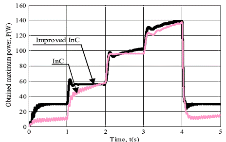
Fig. 4. Obtained maximum output power with the InC and improved InC algorithms under the variation of the solar irradiation.


Fig. 5. Obtained maximum output power with the P&O and improved InC algorithms under both the variations of the solar irradiation and temperature.

Fig. 6. Obtained maximum output power with the InC and improved InC algorithms under both the variations of the solar irradiation and temperature.


Fig. 7. MPPs of the solar PV panel under the variation of the solar irradiation


Fig. 8. MPPs of the solar PV panel under both the variations of the solar irradiation and temperature.


Fig. 9. Experimental result of obtained maximum output power with the improved InC algorithm under the variation of the solar irradiation.

CONCLUSION:
It is obvious that the adaptive and optimal control strategy plays an important role in the development of solar PV systems. This strategy is based on the combination between the ST and MPPT in order to ensure that the solar PV panel is capable of harnessing the maximum solar energy following the sun’s trajectory from dawn until dusk and is always operated at the MPPs with the improved InC algorithm. The proposed InC algorithm improves the conventional InC algorithm with an approximation which reduces the computational burden as well as the application of the CV algorithm to limit the search space and increase the convergence speed of the InC algorithm. This improvement overcomes the existing drawbacks of the InC algorithm. The simulation and experimental results confirm the validity of the proposed adaptive and optimal control strategy in the solar PV panel through the comparisons with other strategies.
REFERENCES:
[1] R. Faranda and S. Leva, “Energy comparison of MPPT techniques for PV systems,” WSES Trans. Power Syst., vol. 3, no. 6, pp. 446–455, 2008.
[2] X. Jun-Ming, J. Ling-Yun, Z. Hai-Ming, and Z. Rui, “Design of track control system in PV,” in Proc. IEEE Int. Conf. Softw. Eng. Service Sci., 2010, pp. 547–550.
[3] Z. Bao-Jian, G. Guo-Hong, and Z. Yan-Li, “Designment of automatic tracking system of solar energy system,” in Proc. 2nd Int. Conf. Ind. Mechatronics Autom., 2010, pp. 689–691.
[4] W. Luo, “A solar panels automatic tracking system based on OMRON PLC,” in Proc. 7th Asian Control Conf., 2009, pp. 1611–1614.
[5] W. Chun-Sheng,W. Yi-Bo, L. Si-Yang, P. Yan-Chang, and X. Hong-Hua, “Study on automatic sun-tracking technology in PV generation,” in Proc. 3rd Int. Conf. Elect. Utility Deregulation Restruct. Power Technol., 2008, pp. 2586–2591.

Novel Cascaded Switched-Diode Multilevel Inverter for Renewable Energy Integration


ABSTRACT:
In this paper, a new topology of two-stage cascaded switched-diode (CSD) multilevel inverter is proposed for medium voltage renewable energy integration. First, it aims to reduce the number of switches along with its gate drivers. Thus, the installation space and cost of a multilevel inverter are reduced. The spike removal switch added in the first stage of the inverter provides a flowing path for the reverse load current, and as a result, high voltage spikes occurring at the base of the stepped output voltage based upon conventional CSD multilevel inverter topologies are removed. Moreover, to resolve the problems related to dc source fluctuations of multilevel inverter used for renewable energy integration, the clock phase-shifting (CPS) one-cycle control (OCC) is developed to control the two-stage CSD multilevel inverter. By shifting the clock pulse phase of every cascaded unit, the staircase-like output voltage waveforms are obtained and a strong suppression ability against fluctuations in dc sources is achieved. Simulation and experimental results are discussed to verify the feasibility and performances of the two-stage CSD multilevel inverter controlled by the CPS OCC method.
KEYWORDS:
1.      Novel cascaded multilevel inverter
2.      Two-stage
3.      One-cycle control

SOFTWARE: MATLAB/SIMULINK

BLOCK DIAGRAM:


Fig. 1. Renewable energy generation system with multilevel inverter.


EXPECTED SIMULATION RESULTS:


Fig. 2. The output voltage and current of the first stage converter of the 5-level
simulation prototype. (a) Output voltage ug ; (b) Output current ig .


Fig. 3. The output voltage and inductor current of the 5-level simulation
prototype. (a) Output voltage uCD ; (b) Output voltage after filter uo ; (c) Inductor current il


Fig. 4. The output voltage and current of the first stage converter of the
9-level simulation prototype. (a) Output voltage ug ; (b) Output current ig .


Fig. 5. The output voltage and inductor current of the 9-level simulation
prototype. (a) Output voltage uCD ; (b) Output voltage after filter uo ; (c) Inductor current il .


Fig. 6. The simulation results of the 5-level prototype: DC source with basic
unit 1 contains a 10 Hz ripple with amplitude 16 V. (a) uo using CPS OCC; (b) uo using CPS SPWM.


Fig. 7. The simulation results of the 5-level prototype: DC source with each
basic unit contains a 10 Hz ripple with amplitude 8 V. (a) uo using CPS OCC; (b) uo using CPS SPWM.

CONCLUSION:
A new topology of two-stage CSD multilevel inverter has been proposed in this paper. n cascaded basic units and one spike removal switch form the first stage. Then by adding a full-bridge inverter as the second-stage converter, both of the positive and negative output voltage levels are generated. Since the one full-bridge converter in the output side leads to the restriction on high-voltage applications, the proposed topology is suitable for medium-voltage renewable energy integration. The comparisons with the CHB and cascaded half-bridge topologies show that the CSD topology requires less switches and related gate drivers for realizing Nlevel output voltage. As a result, the installation space and cost of the multilevel inverter are reduced. Meanwhile, the spike removal switch added in the first stage provides a flowing path for the reverse load current under R-L loads, thus, the high voltage spikes, due to the collapsing magnetic field in a very short time interval, are removed. The CPS OCC method, which is composed by n similar but dependent OCC controllers, has been designed and implemented to control the CSD multilevel inverter. Simulation and experimental results demonstrate that, by shifting the clock pulse phase of each cascaded unit, the staircase-like voltage waveforms are obtained. Moreover, to evaluate the performance of CPS OCC, in both the simulation and experiment, the DC sources mixed with low frequency ripples are implemented to simulate the DC supply from renewable energy generations, and the comparative results between CPS OCC and CPS SPWM reveal that CPS OCC possesses a superior ability in suppressing the unbalance or low frequency ripples in DC sources. These results demonstrate that the CPS OCC method can be a substitute for conventional controllers to control multilevel inverters for renewable energy integration with improved control performances.
 REFERENCES:
[1] M. S. B. Ranjiana, P. S. Wankhade, and N. D. Gondhalekar, “A modified cascaded H-bridge multilevel inverter for solar applications,” in Proc. 2014 Int. Conf. Green Comput. Commun. Elect. Eng., 2014, pp. 1–7.
[2] F. S. Kang, S. J. Park, S. E. Cho, C. U. Kim, and T. Ise, “Mutilevel PWM inverters suitable for the use of stand-alone photovoltaic power systems,” IEEE Trans. Energy Convers., vol. 20, no. 4, pp. 906–915, Dec. 2005.
[3] L. V. Nguyen, H.-D. Tran, and T. T. Johnson, “Virtual prototyping for distributed control of a fault-tolerant modular multilevel inverter for photovoltaics,” IEEE Trans. Energy Convers., vol. 29, no. 4, pp. 841–850, Dec. 2014.
[4] J. Rodriguez, J. S. Lai, and F. Z. Peng, “Mutilevel inverters: A survey of topologies, controls, and application,” IEEE Trans. Ind. Electron., vol. 49, no. 4, pp. 724–738, Aug. 2002.
[5] F. Z. Peng and J. S. Lai, “Mutilevel converters—A new breed of power converters,” IEEE Trans. Ind. Appl., vol. 32, no. 3, pp. 509–517, May/Jun. 1996.