ABSTRACT
In single-phase ac high-voltage (HV) battery
chargers, as the input current is enforced to be varying sinusoidally in phase
with the input voltage, the pulsating power at two times of the line frequency
will be seen on the dc-link. Bulky capacitor bank or extra active filter
circuits are needed to assimilate this harmonic current, which become a major
barrier in terms of power density and cost. Sinusoidal charging method can be
applied, while this might affect the charging efficiency and a deep study is still
needed to further investigate on the impact to the Lithium-ion battery. An
active filter auxiliary power module (AFAPM) based dual-mode dual-voltage
charging system for vehicle application has been proposed. The AFAPM converter
has two modes: 1) the HV active filtering mode, in which the vehicle is
connected to the grid and the converter assimilates the significant
second-order harmonic current; 2) the low-voltage (LV) battery charging mode,
in which the vehicle is running and the converter charges the LV battery from
HV battery. However, a relay and inductors are still required in that converter
to achieve the dual-mode operation. This paper proposes a primary
full-integrated AFAPM for electrified vehicle applications with single-phase
onboard chargers. The proposed AFAPM converter is composed of a two-phase
bidirectional buck converter to work as an active filter (AF) and a
dual-active-bridge (DAB) to operate as a LV battery charger auxiliary power
module (APM). With the proposed converter, only an extra active energy storage
capacitor is needed to achieve the active filtering. All the switches and
inductors on the primary stage are shared between the AF and APM. Therefore,
the use of a bulky capacitor bank or an additional AF circuit is avoided and
thus, the cost, size and weight of the dual-voltage charging system in the
electrified vehicle applications can be reduced. To confirm the effectiveness
of the proposed converter, a 720 W prototype.
KEYWORDS:
1. Active filters, auxiliary power modules
2. Dc/Dc converters
3. Dual-voltage charging systems
4. Plug-in hybrid electric vehicles
5. Single-phase chargers.
SOFTWARE: MATLAB/SIMULINK
CIRCUIT
DIAGRAM:

Fig. 1: The dual-voltage charging
system with the proposed primary full-integrated AFAPM.
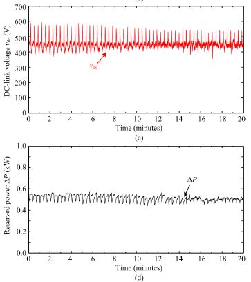
EXPECTED SIMULATION RESULTS:

Fig. 2: Simulation results of AF mode, (a) HV
dc-link voltage vdc, (b) capacitor Cr voltage
vcr, (c) transformer primary voltage vpri,
(d) inductor Lra and Lrb current ira
and irb, (e) capacitor Cr current icr.

Fig. 3: Simulation results of APM mode, (a)
transformer primary voltage vpri, (b) transformer secondary
voltage vsec, (c) inductor Lra and Lrb
current ira and irb, (d) LV output
current iLo, (e) capacitor Cr voltage vcr
CONCLUSION
In this paper, a
new primary full-integrated AFAPM converter is proposed. The proposed converter
is not only a LV battery charger APM, but also an AF for the HV battery
charger. A full bridge and auxiliary inductors are shared between the DAB APM
converter and the two phase buck AF converter. Only an active harmonic energy
storage capacitor is needed to achieve active filtering. As a result, from the
harmonic energy storage aspect for the 6.6 kW HV battery charger in the vehicle
applications, with the proposed AFAPM method, the volume and cost can decrease
to 45.8% and 44.7% of the volume and cost of the conventional extra active
filter method, respectively. A 720 W
prototype has been built and experiments show promising results confirming the
effectiveness of the proposed converter.
REFERENCES
.
[1]
L. Xue, Z. Shen, D. Boroyevich, P. Matavelli,
and D. Diaz, “Dual active bridge-based battery charger for plug-in hybrid
electric vehicle with charging current containing low frequency ripple,” IEEE
Transactions on Power Electronics, vol. 30, no. 12, pp. 7299-7307, Dec.
2015.
[2]
B. Bilgin, P. Magne, P. Malysz, Y. Yang, V.
Pantelic, M. Preindl, A. Korobkine, W. Jiang, M. Lawford, and A. Emadi, “Making
the case for electrified transportation,” IEEE Transactions on
Transportation Electrification, vol. 1, no. 1, pp. 4-17, Jun. 2015.
[3]
S. Jahdi, O. Alatise, C. Fisher, R. Li, and P.
Mawby, “An evaluation of silicon carbide unipolar technologies for electric
vehicle drive-trains,” IEEE Journal of Emerging and Selected Topics in Power
Electronics, vol. 2, no. 3, pp. 517–528, Sep. 2014.
[4]
H. A.
Mantooth, M. D. Glover, and P. Shepherd, “Wide bandgap technologies and their
implications on miniaturizing power electronic systems,” IEEE Journal of
Emerging and Selected Topics in Power Electronics, vol. 2, no. 3, pp.
374-385, Sep. 2014.