asokatechnologies@gmail.com 09347143789/09949240245

Search This Blog

Monday, 15 May 2017

Full Soft-Switching High Step-Up Dc-Dc Converter For Photovoltaic Applications


 ABSTRACT:
In this paper a full soft-switching high step-up DC-DC converter is introduced as an alternative approach to module integrated converters for photovoltaic applications. The presented operation principle and key equations can be used as design guidelines for component and parameter estimation in practical applications. The proposed DC-DC converter was verified by help of simulations and experiments. Power loss analysis based on the semiconductor datasheet values showed that the converter tends to achieve an efficiency of 92. 8% at the maximum power point.

KEYWORDS:
1.      DC-DC power conversion
2.       Photovoltaic power systems
3.       MOSFET switches

SOFTWARE: MATLAB/SIMULINK

CIRCUIT DIAGRAM:


Fig. 1: Generalised topology of the proposed DC-DC converter.

EXPECTED SIMULATION RESULTS:


Fig. 2: Simulated voltage and current waveforms of MOSFET SI (a), MOSFET Tl (b), transformer
primary (c) as well as the input and output voltage and current waveforms (d).


Fig. 3: Converter regulation characteristics at different irradiation levels (a) and cell temperatures (b).

Fig. 4: Experimental voltage and current waveforms of Tl MOSFET (a), SI MOSFET (b) and S2
MOSFET (c).


Fig. 5: Experimental waveforms of the input (a) and output (b) voltage and current.

CONCLUSION:

The proposed high step-up DC-DC converter allows ZVS of the inverter switches and ZCS of the rectifier switches. The operation principle presented and the mathematical analysis of the converter can be used as design guidelines for component and parameter estimation in practical applications. The operation of the converter was verified with the 300 W experimental prototype and the experimental waveforms were found to correspond to the estimated ones. The major limitation of the converter lies in the diodes connected in series to the inverter transistors. The static losses in these diodes will contribute a major portion of the total converter losses. In the future these diodes will be replaced by MOSFETs, external snubber capacitors for rectifier switches will be introduced and the implementation possibilities of wide-bandgap semiconductors will be also addressed.

REFERENCES:

[1] Walker, G.R.; Sernia, P.C., "Cascaded DC-DC converter connection of photo voltaic modules", 33rd Annual Power Electronics Specialists Conference PESC'2002, vol. I, pp.24-29, 2002.
[2] Forcan, M.; Tusevljak, J.; Lubura, S.; Soja, M., "Analyzing and Modeling the Power Optimizer forBoosting Efficiency of PV Panel", IX Symposium Industrial Electronics INDEL'2012, pp. 198-193, Banja Luka, November 01-03,2012.
[3] Kasper, M.; Bortis, D.; Friedli, T.; Kolar, J.W., "Classification and comparative evaluation of PV panel integrated DC-DC converter concepts," Power Electronics and Motion Control Conference (EPEIPEMC), 2012 15th International, pp.LSle.4-1,LSle.4-8, 4-6 Sept. 2012.
[4] Christian Peter Dick "Multi-Resonant Converters as Photovoltaic Module-Integrated Maximum Power Point Tracker", PhD Thesis 2010, available: http://darwin.bth.rwth-aachen.de/opus3/volltexte/20 1 0/3267 /pdf/3267 .pdf

[5] Kasper, Matthias; Ritz, Magdalena; Bortis, Dominik; Kolar, Johann W., "PV Panel-Integrated High Step-up High Efficiency Isolated GaN DC-DC Boost Converter," Proceedings of 2013 35th International Telecommunications Energy Conference 'Smart Power and Efficiency' (INTELEC), pp.I-7, 13 17 Oct. 2013.

Zero-Voltage Switching Galvanically Isolated Current-Fed Full-Bridge DC-DC Converter


ABSTRACT:
This paper presents a new soft-switching technique for the current-fed full-bridge DC-DC converter that enables zero voltage switching of the input side inverter switches. To achieve this, the secondary side voltage doubler rectifier has to be realized with active switches. Two control channels synchronous with the control signals of the inverter switches are added for driving those switches. Zero voltage switching achieved is assisted with the body diodes that conduct current during soft-switching transients as a result of the leakage inductance current shaping from the secondary side. Moreover, the converter does not suffer from voltage overshoots thanks to natural clamping from the secondary side. Theoretical predictions were verified with simulation.

KEYWORDS:
1.      Zero-voltage switching
2.      Current-fed DC-DC converter
3.      Full-bridge
4.      Soft-switching
5.      Switching` control method

SOFTWARE: MATLAB/SIMULINK

 CIRCUIT DIAGRAM:


 Fig. 1. Galvanically isolated full-bridge current-fed DC-DC converter with controlled output rectifier stage.


 EXPECTED SIMULATION RESULTS:


Fig. 2. Simulated current and voltage waveforms along with control signals
of the input and output side switches.


Fig. 3. Experimental current and voltage waveforms.

CONCLUSION:

The novel ZVS technique intended for the galvanically isolated full-bridge current-fed DC-DC converter with the controlled output rectifier stage were presented. It enables full ZVS in the input side current-fed inverter assisted with the leakage inductance and body diodes. Moreover, partial ZCS is provided in the secondary side assisted with the leakage inductance. Simulation study corroborates the theoretical predictions made. Experimental prototype operation was quite similar to the simulation model created in PSIM. Nevertheless, the prototype features oscillations caused by parasitic elements of the circuit and reverse recovery of the body diodes the input side MOSFETs. Further research will be aimed towards derivation of design guidelines that take into account reverse recovery effect and, consequently, result in high efficiency and low parasitic oscillations.

REFERENCES:

[1] Blaabjerg, F.; Zhe Chen; Kjaer, S.B., "Power electronics as efficient interface in dispersed power generation systems," IEEE Transactions on Power Electronics, vol. 19, no. 5, pp. 1184-1194, Sept. 2004.
[2] Kouro, S.; Leon, J.I.; Vinnikov, D.; Franquelo, L.G., "Grid-Connected Photovoltaic Systems: An Overview of Recent Research and Emerging PV Converter Technology," IEEE Industrial Electronics Magazine, vol. 9, no. 1, pp. 47-61, March 2015.
[3] Rathore, A.K.; Prasanna, U., "Comparison of soft-switching voltage-fed and current-fed bi-directional isolated Dc/Dc converters for fuel cell vehicles," in Proc. ISIE’2012, pp. 252-257, 28-31 May 2012.
[4] Prasanna, U.R.; Rathore, A.K., "Extended Range ZVS Active-Clamped Current-Fed Full-Bridge Isolated DC/DC Converter for Fuel Cell Applications: Analysis, Design, and Experimental Results," IEEE Transactions on Industrial Electronics, vol. 60, no. 7, pp. 2661-2672, July 2013.

[5] Iannello, C.; Shiguo Luo; Batarseh, I., "Small-signal and transient analysis of a full-bridge, zero-current-switched PWM converter using an average model," IEEE Transactions on Power Electronics, vol.18, no.3, pp.793-801, May 2003.

Analysis and Control of Isolated Current-fed Full Bridge Converter in Fuel Cell System


 ABSTRACT:

Fuel cells are considered as one of the most prominent sources of green energy in future. However, the potential efficiency of fuel cell will he untapped unless an efficient method can be used to Convert the fuel cell low voltage to high voltage grid or user load. Many topologies have been proposed for such applications. However, most of them consider the fuel cell as an voltage source instead of a current source. In this paper, an isolated current-fed full bridge boost converter is proposed as the front end of the fuel cell system, which is more compatible with the fuel cell particularities. Small signal analysis is applied to the compiler and current control method is used. Simulation and experiment results are shown to ,verify the analysis.


SOFTWARE: MATLAB/SIMULINK

CIRCUIT DIAGRAM:


Fig. 1. (a) Conventional full bridge current-fed convener; (b) Proposed full
bridge current·fed boost converter


EXPECTED SIMULATION RESULTS:


Fig. 2. Main wavefonns of the proposed converter (simulated)


Fig. 3. Main waveforms of the proposed converter when Vg = 5V. IL = 6A
(experiment)

Fig. 4. Output voltage and inductor current with PI voltage control (simulated)


Fig. 5. Output voltage and inductor current with current control (simulated)

Fig. 6. Output voltage and inductor current with current control during load
changing (experiment)

CONCLUSION:

In order to speed up the market acceptance of EVs/HEVs, the capital cost in charging infrastructure needs to lower as much as possible. This paper has presented an improved asymmetric half-bridge converter-fed SRM drive to provide both driving and on-board DC and AC charging functions so that the reliance on off-board charging stations is reduced.  The main contributions of this paper are: (i) it combines the split converter topology with central tapped SRM windings to improve the system reliability. (ii) the developed control strategy enables the vehicle to be charged by both DC and AC power subject to availability of power sources. (iii) the battery energy balance strategy is developed to handle unequal SoC scenarios. Even through a voltage imbalance of up to 20% in the battery occurs, the impact on the driving performance is rather limited. (iv) the state-of-charge of the batteries is coordinated by the hysteresis control to optimize the battery performance; the THD of the grid-side current is 3.7% with a lower switching frequency.  It needs to point out that this is a proof-of-concept study based on a 150 W SRM and low-voltage power for simulation and experiments. In the further work, the test facility will be scaled up to 50 kW.

REFERENCES:

[1] B. K. Bose, “Global energy scenario and impact of power electronics in 21st Century,” IEEE Trans. Ind. Electron., vol. 60, no. 7, pp. 2638- 2651, Jul. 2013.
[2] J. de Santiago, H. Bernhoff, B. EkergÃ¥rd, S. Eriksson, S. Ferhatovic, R. Waters, and M. Leijon, “Electrical motor drivelines in commercial all-electric vehicles: a review,” IEEE Trans. Veh. Technol., vol. 61, no. 2, pp. 475-484, Feb. 2012.
[3] A. Chiba, K. Kiyota, N. Hoshi, M. Takemoto, S. Ogasawara, “Development of a rare-earth-free SR motor with high torque density for hybrid vehicles,” IEEE Trans. Energy Convers., vol. 30, no. 1, pp.175-182, Mar. 2015.
[4] K. Kiyota, and A. Chiba, “Design of switched reluctance motor competitive to 60-Kw IPMSM in third-generation hybrid electric vehicle,” IEEE Trans. Ind. Appl., vol. 48, no. 6, pp. 2303-2309, Nov./Dec. 2012.

[5] S. E. Schulz, and K. M. Rahman, “High-performance digital PI current regulator for EV switched reluctance motor drives,” IEEE Trans. Ind. Appl., vol. 39, no. 4, pp. 1118-1126, Jul./Aug. 2003.

Residential Photovoltaic Energy Storage System


ABSTRACT:
This paper introduces a residential photovoltaic (PV) energy storage system, in which the PV power is controlled by a dc–dc converter and transferred to a small battery energy storage system (BESS). For managing the power, a pattern of daily operation considering the load characteristic of the homeowner, the generation characteristic of the PV power, and the power leveling demand of the utility is prescribed. The system looks up the pattern to select the operation mode, so that powers from the PV array, the batteries, and the utility are utilized in a cost-effective manner. As for the control of the system, a novel control technique for the maximum power-point tracking (MPPT) of the PV array is proposed, in which the state-averaged model of the dc–dc converter, including the dynamic model of the PV array, is derived. Accordingly, a high-performance discrete MPPT controller that tracks the maximum power point with zero-slope regulation and current-mode control is presented. With proposed arrangements on the control of the BESS and the current-to-power scaling factor setting, the dc–dc converter is capable of combining with the BESS for performing the functions of power conditioning and active power filtering. An experimental 600-W system is implemented, and some simulation and experimental results are provided to demonstrate the effectiveness of the proposed system.
KEYWORDS:
1.      Active power filtering
2.       Battery energy storage system
3.       Maximum power-point tracking
4.       Power conditioning

SOFTWARE: MATLAB/SIMULINK

CIRCUIT DIAGRAM:


Fig. 1. The power circuit of proposed PV energy storage system.

EXPECTED SIMULATION RESULTS:


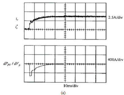
Fig. 2. Simulated results of MPPT control. (a) An increasing step change in Ip. (b) A decreasing step change in Ip.

 Fig. 3. Measured waveforms of , andin MPPT control.


Fig. 4. System operations. (a) Measured waveforms when system is changed from mode 3 to mode 2, where subscripts o;L; and u are used to represent the BESS, the load, and the utility, respectively. (b) Measured real power waveforms in various operation modes.

CONCLUSION:
This paper has proposed a residential PV energy storage system, where the PV power is controlled by a dc–dc converter and transferred to a small BESS. The proposed system, possessing the functions of power conditioner and active power filter, is capable of providing an optimal interface with the utility. The additional PV power makes the system flexible in power usage, so that all powers in the system can be utilized in a cost-effective manner. Some control techniques for realizing the functions of the proposed system, including the MPPT control of the PV array and control of power flows in the system, have been presented. A prototype 600-W system was implemented, and some simulated and experimental results were provided to demonstrate the effectiveness of the proposed system. Although the setup cost of the proposed system is high, such that it is hard to compete with the current utility power, we believe that the capital issue will be resolved if there is a political encouragement in the kilowatt price and the market is large enough.

REFERENCES:
[1] G. J. Jones, “The design of photovoltaic systems for residential applications,” in Conf. Rec. IEEE Photovoltaic Specialists Conf., 1981, pp. 805–810.
[2] G. L. Campen, “An analysis of the harmonics and power factor effects at a utility intertied photovoltaic system,” IEEE Trans. Power App. Syst., vol. PAS-101, pp. 4632–4639, Dec. 1982.
[3] C. M. Liaw, T. H. Chen, S. J. Chiang, C. M. Lee, and C. T. Wang, “Small battery energy storage system,” Proc. Inst. Elect. Eng., vol. 140, pt. B, no. 1, pp. 7–17, 1993.
[4] S. J. Chiang, “Design and implementation of multi-functional battery energy storage systems,” Ph.D. dissertation, Dep. Elect. Eng., National Tsing Hua University, Hsin-Chu, Taiwan, R.O.C., 1994.

[5] Z. Salameh and D. Taylor, “Step-up maximum power point tracker for photovoltaic arrays,” Sol. Energy Proc., vol. 44, no. 1, pp. 57–61, 1990.

Novel Zero-Current Switching Current-Fed Half-Bridge Isolated Dc/Dc Converter for Fuel Cell Based Applications


ABSTRACT:
This paper presents a novel zero-current switching (ZCS) current-fed half-bridge isolated dc/dc converter. It is a potential topology for front-end dc/dc power conversion for fuel cell inverters. This proposed converter is unique, not reported in literature and provides a simple solution to switch turn-off problem with ZCS without increase in components count. This will lead to reduced size, lower cost and higher efficiency. Analysis, design and simulation results of the proposed converter are reported in this paper. A comparison with existing active-clamped ZVS current-fed half-bridge converter has been illustrated.

KEYWORDS:
1.      Zero-current switching
2.      Dc/Dc converter
3.      Current-fed
4.      Fuel cells
5.      High efficiency

SOFTWARE: MATLAB/SIMULINK

 BLOCK DIAGRAM:
Fig. 1. Conventional hard-switched current-fed half-bridge dc/dc converter

Fig. 2 Active-clamped ZVS current-fed half-bridge dc/dc converter

Fig. 3. Proposed ZCS current-fed half-bridge dc/dc converter.


 EXPECTED SIMULATION RESULTS:

Fig. 4. Zero-current switching of primary-side switches. The ripple frequency of input current Iin is 200 kHz, which
is same twice the switching frequency fs. The transformer

Fig. 5. Zero-current turn-on of primary-side switches. V(S1) is voltage across switch S1 and I(S1) is current through switch S1. The current waveform is scaled for clarity.

Fig. 6. Current-waveforms through the secondary-side switches.

Fig. 7. Zero-current turn-on of secondary-side switches. V(Sr1) is voltage across switch Sr1 and I(Sr1) is current through switch S\r1. The current waveform is scaled for clarity.
Fig. 8. Current waveforms through input inductors L1 and L2.
Fig. 9. . Input current (Iin) and transformer current I(Ls) waveforms.

REFERENCES:
[1] www.fossil.gov.in
[2] S. K. Mazumder, R. K. Burra, and K. Acharya, “A ripple-mitigating and energy-efficient fuel cell power-conditioning system,” IEEE Transactions on Power Electronics, vol. 22, 2007, pp. 1437-1452.
[3] Jin-Tae Kim, Byoung-Kuk Lee, Tae-Won Lee, Su-Jin Jang, Soo-Seok Kim, and Chung-Yuen Won, “An active clamping current-fed half bridge converter for fuel-cell generation systems,” in Proceedings 2004 IEEE Power Electronics Specialists Conference, pp. 4709-4714.
[4] S. Han, H. Yoon, G. Moon, M. Youn, Y. Kim, and K. Lee, “A new active-clamping zero-voltage switching PWM current-fed half-bridge converter,” IEEE Transactions on Power Electronics, vol. 20, pp 1271- 1279, 2006.

[5] S. J. Jang, C. Y. Won, B. K. Lee and J. Hur, “Fuel cell generation system with a new active clamping current-fed half-bridge converter,” IEEE Trans. on Energy Conversion, vol. 22, pp. 332-340, June 2007.