asokatechnologies@gmail.com 09347143789/09949240245

Search This Blog

Sunday, 26 August 2018

An Enhanced Voltage Sag Compensation Scheme for Dynamic Voltage Restorer

IEEE Transactions on Industrial Electronics, 2013

ABSTRACT
This paper deals with improving the voltage quality of sensitive loads from voltage sags using dynamic voltage restorer (DVR). The higher active power requirement associated with voltage phase jump compensation has caused a substantial rise in size and cost of dc link energy storage system of DVR. The existing control strategies either mitigate the phase jump or improve the utilization of dc link energy by (i) reducing the amplitude of injected voltage, or (ii) optimizing the dc bus energy support. In this paper, an enhanced sag compensation strategy is proposed that mitigates the phase jump in the load voltage while improving the overall sag compensation time. An analytical study shows that the proposed method significantly increases the DVR sag support time (more than 50%) compared with the existing phase jump compensation methods. This enhancement can also be seen as a considerable reduction in dc link capacitor size for new installation. The performance of proposed method is evaluated using simulation study.

KEYWORDS:
1.      Dynamic voltage restorer (DVR)
2.      Voltage source inverter (VSI)
3.      Voltage sag compensation
4.      Voltage phase jump compensation.

SOFTWARE: MATLAB/SIMULINK

BLOCK DIAGRAM:

Fig. 1. Basic DVR based system configuration

EXPECTED SIMULATION RESULTS:

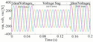
Fig. 2. Simulation results for the proposed sag compensation method for 50% sag depth. (a) PCC voltage, (b) load voltage, (c) DVR voltage, (d) DVR active and reactive power, and (e) dc link voltage.

Fig. 3. Simulation results for the proposed sag compensation method for 23% sag depth. (a) PCC voltage, (b) load voltage, (c) DVR voltage, (d) DVR active and reactive power, and (e) dc link voltage.

CONCLUSION
In this paper an enhanced sag compensation scheme is proposed for capacitor supported DVR. The proposed strategy improves the voltage quality of sensitive loads by protecting them against the grid voltage sags involving the phase jump. It also increases compensation time by operating in minimum active power mode through a controlled transition once the phase jump is compensated. To illustrate the effectiveness of the proposed method an analytical comparison is carried out with the existing phase jump compensation schemes. It is shown that compensation time can be extended from 10 to 25 cycles (considering pre sag injection as the reference method) for the designed limit of 50% sag depth with 450 phase jump. Further extension in compensation time can be achieved for intermediate sag depths. This extended compensation time can be seen as considerable reduction in dc link capacitor size (for the studied case more than 50%) for the new installation. The effectiveness of the proposed method is evaluated through extensive simulations in MATLAB/Simulink and validated on a scaled lab prototype experimentally. The experimental results demonstrate the feasibility of the proposed phase jump compensation method for practical applications.

REFERENCES

[1]   J.A. Martinez and J.M. Arnedo, “Voltage sag studies in distribution networks- part I: System modeling,” IEEE Trans. Power Del., vol. 21,no. 3, pp. 338–345, Jul. 2006.
[2]   J.G. Nielsen, F. Blaabjerg and N. Mohan, “Control strategies for dynamic voltage restorer, compensating voltage sags with phase jump,” in Proc. IEEE APEC, 2001, pp. 1267–1273.
[3]   J.D. Li, S.S. Choi, and D.M. Vilathgamuwa, “Impact of voltage phase jump on loads and its mitigation,” in Proc. 4th Int. Power Electron. Motion Control Conf., Xian, China, Aug. 14–16, 2004, vol. 3, pp. 1762– 176.
[4]   M. Sullivan, T. Vardell, and M. Johnson, “Power interruption costs to industrial and commercial consumers of electricity, IEEE Trans. Ind App., vol. 33, no. 6, pp. 1448–1458, Nov. 1997.
[5]   J. Kaniewski, Z. Fedyczak and G. Benysek "AC Voltage Sag/Swell Compensator Based on Three-Phase Hybrid Transformer With Buck- Boost Matrix-Reactance Chopper", IEEE Trans. Ind. Electron., vol.61, issue. 8, Aug 2014.

Saturday, 25 August 2018

Time-Varying and Constant Switching Frequency Based Sliding Mode Control Methods for Trans- former less DVR Employing Half-Bridge VSI


IEEE Transactions on Industrial Electronics, 2016


 ABSTRACT:
This paper presents time-varying and constant switching frequency based sliding mode control (SMC) methods for three-phase transformerless dynamic voltage restorers (TDVRs) which employ half-bridge voltage source inverter (VSI). An equation is derived for the time-varying switching frequency. However, since the time-varying switching frequency is not desired in practice, a smoothing operation is applied to the sliding surface function within a narrow boundary layer with the aim of eliminating the chattering effect and achieving a constant switching frequency operation. The control signal obtained from the smoothing operation is compared with a triangular carrier signal to produce the PWM signals. The feasibility of both SMC methods has been validated by experimental results obtained from a TDVR operating under highly distorted grid voltages and voltage sags. The results obtained from both methods show excellent performance in terms of dynamic response and low total harmonic distortion (THD) in the load voltage. However, the constant switching frequency based SMC method not only offers a constant switching frequency at all times and preserves the inherent advantages of the SMC, but also leads to smaller THD in the load voltage than that of time-varying switching frequency based SMC method.

KEYWORDS:
1.        Constant switching frequency
2.        Dynamic voltage restorer
3.        Sliding mode control
4.        Time-varying switching frequency.

SOFTWARE: MATLAB/SIMULINK

BLOCK DIAGRAM:
Fig. 1. Block diagram of three-phase TDVR with the proposed SMC methods. (a) Time-varying switching frequency based SMC method, (b) Constant switching frequency based SMC method.

EXPECTED SIMULATION RESULTS:


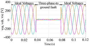
Fig.2. Simulated responses of sk v , se k v , and Lk v obtained by the constant switching frequency based SMC under three-phase-to-ground fault. (a) sk v , (b) se k v , and (c)Lk v .


Fig. 3. Simulated responses of vsk , se k v , and Lk v obtained by the constant switching frequency based SMC under single-phase-to-ground fault. (a)sk v , (b) se k v , and (c)Lk v .


Fig. 4. Simulated responses of sk v , se k v , and Lk v obtained by the SMC method presented in [15]. (a) sk v , (b) se k v , and (c) Lk


Fig. 5. Simulated responses of sk v , se k v , and Lk v obtained by the time-varying switching frequency based SMC. (a) sk v , (b) se k v , and (c)Lk v .


Fig. 6. Simulated responses of sk v , se k v , and Lk v obtained by the constant switching frequency based SMC. (a) sk v , (b) se k v , and (c)Lk v .

CONCLUSION:
In this study, time-varying and constant switching frequency based SMC methods are presented for three-phase TDVR employing half-bridge VSI. An analytical equation is derived to compute the time-varying switching frequency. Since, the time-varying switching frequency is not desired in a real application, a smoothing operation is applied to the sliding surface function within a narrow boundary layer with the aim of eliminating the chattering effect and achieving a constant switching frequency. The control signal obtained from the smoothing operation is compared with a triangular carrier signal to produce the PWM signals. It is observed that the smoothing operation results in a constant switching frequency operation at all times. The feasibility of both SMC methods has been validated by experimental results obtained from the TDVR operating under highly distorted grid voltages and voltage sags. The results obtained from both methods show excellent performance. However, the constant switching frequency based SMC method not only offers a constant switching frequency at all times and preserves the inherent advantages of the SMC, but also leads to smaller THD in the load voltage than that of time-varying switching frequency based SMC method.

REFERENCES:
[1]   M. Bollen, Understanding Power Quality Problems. New York, NY, USA: IEEE Press, 2000.
[2]   B. Singh, A. Chandra, and K. Al-Haddad, Power Quality: Problems and Mitigation Techniques. West Sussex, United Kingdom: John Wiley & Sons Inc., 2015.
[3]   Y. W. Li, F. Blaabjerg, D. M. Vilathgamuwa, and P. C. Loh, ”Design and comparison of high performance stationary-frame controllers for DVR implementation,” IEEE Trans. Power Electron., vol. 22, no. 2, pp. 602-612, Mar. 2007.
[4]   H. Kim, and S. K. Sul, ”Compensation voltage control in dynamic voltage restorers by use of feed forward and state feedback scheme,” IEEE Trans. Power Electron., vol. 20, no. 5, pp. 1169-1177, Sep. 2005.

Multilevel Cascaded-TypeDynamic Voltage Restorer with Fault Current Limiting Function


IEEE Transactions on Power Delivery, 2015

ABSTRACT:
This paper presents a new multilevel cascaded-type dynamic voltage restorer (MCDVR) with fault current limiting function. This topology can operate in two operational modes: 1) compensation mode for voltage fluctuations and unbalances, and 2) short-circuit current limiting mode. The current limiting function of the MCDVR is performed by activating anti-parallel thyristors during the short-circuit fault, and deactivating them during normal operation. The mathematical model of the MCDVR system is also established in this paper. The control scheme design and optimal parameter selection are outlined based on the detailed theoretical analysis of the converter. The transient states of the MCDVR in both the compensation mode and current-limiting mode are also analyzed. Simulation results based on the PSCAD/EMTDC software and experimental results on a laboratory setup help to validate the proposed topology and the theoretical analysis.

KEYWORDS:
1.      Dynamic voltage restorer (DVR)
2.      Multilevel inverters
3.      Fault current limiter
4.      Voltage restoration

SOFTWARE: MATLAB/SIMULINK

BLOCK DIAGRAM:


Fig. 1. Schematic diagram of the proposed MCDVR.


 EXPECTED SIMULATION RESULTS:
Fig. 2. Simulation results of the MCDVR system. Top to bottom: (a) the supply voltage Us, (b) the load voltage UL, (c) the secondary voltage Udvr, (d) the load current IL, and (e) the dc-link voltage.

Fig. 3. Forward switching simulations of the MCDVR system, top to bottom: (a) the load current IL, (b) the current Iscr in the thyristor’s path, (c) the output current Idvr of the VSI, (d) the dc-link voltage Udc, and (e) the timing sequence

Fig. 4. Backward switching simulations of the MCDVR system, top to bottom: (a) the load current IL, (b) the current Iscr in the thyristor’s path, (c) the output current Idvr of the VSI, (d) the dc-link voltage Udc, and (e) the timing sequence.

CONCLUSION:
Cascaded multilevel inverters have been applied in the industry as a cost-effective means of series sag compensation. However, a large current will be induced into the VSI through a series transformer during faults, and this is harmful to the VSI and the other equipment in the grid. In this paper, the MCDVR was proposed to deal with voltage sags and short-circuit current faults. The MCDVR has not only the advantages of the H-bridge cascade inverter, but also reduces the secondary side current in the preliminary period of the fault. A mathematical model of this system was also established in this paper. A careful analysis of the transient state verified the feasibility of the proposed MCDVR. Based on the theoretical analysis, PSCAD/EMTDC simulations and the experimental results, we can conclude the following:
1) The H-bridge cascade inverter can be adopted to reduce the series transformation ratio and the secondary current during the preliminary period of the fault.
2) The transient state of the MCDVR system was introduced in great detail.
3) The proposed control method can limit fault current with two cycle. The consistencies between the simulation results and experimental results help to verify the proposed topology and theoretical analysis.

REFERENCES:
[1]         C.-S. Lam, M-C. Wong, and Y.-D. Han, “Voltage swell and overvoltage compensation with unidirectional power flow controlled dynamic voltage restorer,” IEEE Trans. Power Del., vol. 23, no. 4, pp. 2513-2521, Oct. 2008.
[2]         M. Jafari, S. B. Naderi, M. Tarafdar Hagh, M. Abapour, and S. H. Hosseini, “Voltage sag compensation of point of common coupling (PCC) using fault current limiter,” IEEE Trans. Power Del., vol. 26, no. 4, pp. 2638-2646, Oct. 2011.
[3]         F. Z. Peng and J. S. Lai, “A multilevel voltage-source converter with separate DC source for static var generation,” IEEE Trans. Ind. Applicat., vol. 32, no. 5, pp. 1130-1138, Sep./Oct. 1996.
[4]         H. K. Al-Hadidi, A. M. Gole, and D. A. Jacobson, “Minimum power operation of cascade inverter-based dynamic voltage restorer,” IEEE Trans. Power Del., vol. 23, no. 2, pp. 889-898, Apr. 2008.

Integrated Photovoltaic and Dynamic Voltage Restorer System Configuration


IEEE TRANSACTIONS ON SUSTAINABLE ENERGY, 2015

ABSTRACT:
This paper presents a new system configuration for integrating a grid-connected photovoltaic (PV) system together with a self-supported dynamic voltage restorer (DVR). The proposed system termed as a “six-port converter,” consists of nine semiconductor switches in total. The proposed configuration retains all the essential features of normal PV and DVR systems while reducing the overall switch count from twelve to nine. In addition, the dual functionality feature significantly enhances the system robustness against severe symmetrical/asymmetrical grid faults and voltage dips. A detailed study on all the possible operational modes of six-port converter is presented. An appropriate control algorithm is developed and the validity of the proposed configuration is verified through extensive simulation studies under different operating conditions.

KEYWORDS:
1.      Bidirectional power flow
2.      Distributed power generation
3.      Photovoltaic (PV) systems
4.      Power quality
5.      Voltage control

SOFTWARE: MATLAB/SIMULINK

BLOCK DIAGRAM:


Fig. 1. Proposed integrated PV and DVR system configuration.

 EXPECTED SIMULATION RESULTS:

Fig. 2. Simulation results: operation of proposed system during health grid mode (PV-VSI: active and DVR-VSI: inactive). (a) Vpcc; (b) PQload; (c) PQgrid; (d) PQpv-VSI; and (e) PQdvr-VSI.

Fig. 3. Simulation results: operation of proposed system during fault mode (PV-VSI: inactive and DVR-VSI: active). (a) Vpcc; (b) Vdvr; (c) Vload; (d) PQload; (e) PQgrid; (f) PQpv-VSI; and (g) PQdvr-VSI.

Fig. 4. Simulation results: operation of proposed system during balance three phase sag mode (PV-VSI: active and DVR-VSI: active). (a) Vpcc; (b) Vdvr-VSI; (c) Vload; (d) PQgrid; (e) PQpv-VSI; and (f) PQdvr-VSI.

Fig. 5. Simulation results: operation of proposed system during unbalanced sag mode (PV-VSI: active and DVR-VSI: active). (a) Vpcc; (b) Vdvr-vsi; (c) Vload; (d) PQgrid; (e) PQpv-VSI; and (f) PQdvr-VSI.

 
Fig. 6. Simulation results: operation of proposed system during inactive PV plant mode (PV-VSI: active and DVR-VSI: active). (a) Vpcc; (b) Vload; (c) Vdc; (d) PQload; (e) PQdvr-VSI; and (f) PQpv-VSI.


CONCLUSION:
In this paper, a new system configuration for integrating a conventional grid-connected PV system and self supported DVR is proposed. The proposed configuration not only exhibits all the functionalities of existing PV and DVR system, but also enhances the DVR operating range. It allows DVR to utilize active power of PV plant and thus improves the system robustness against sever grid faults. The proposed configuration can operate in different modes based on the grid condition and PV power generation. The discussed modes are healthy grid mode, fault mode, sag mode, and PV inactive mode. The comprehensive simulation study and experimental validation demonstrate the effectiveness of the proposed configuration and its practical feasibility to perform under different operating conditions. The proposed configuration could be very useful for modern load centers where on-site PV generation and strict voltage regulation are required.

REFERENCES:
[1]   R. A. Walling, R. Saint, R. C. Dugan, J. Burke, and L. A. Kojovic, “Summary of distributed resources impact on power delivery systems,” IEEE Trans. Power Del., vol. 23, no. 3, pp. 1636–1644, Jul. 2008.
[2]   C. Meza, J. J. Negroni, D. Biel, and F. Guinjoan, “Energy-balance modeling and discrete control for single-phase grid-connected PV central inverters,” IEEE Trans. Ind. Electron., vol. 55, no. 7, pp. 2734–2743, Jul. 2008.
[3]   T. Shimizu, O. Hashimoto, and G. Kimura, “A novel high-performance utility-interactive photovoltaic inverter system,” IEEE Trans. Power Electron., vol. 18, no. 2, pp. 704–711, Mar. 2003.
[4]   S. B. Kjaer, J. K. Pedersen, and F. Blaabjerg, “A review of single-phase grid-connected inverters for photovoltaic modules,” IEEE Trans. Ind. Appl., vol. 41, no. 5, pp. 1292–1306, Sep./Oct. 2005.