asokatechnologies@gmail.com 09347143789/09949240245

Search This Blog

Monday 27 August 2018

Design Considerations of a Fault Current Limiting Dynamic Voltage Restorer (FCL-DVR)


IEEE TRANSACTIONS ON SMART GRID, 2014

ABSTRACT
This paper proposes a new fault current limiting dynamic voltage restorer (FCL-DVR) concept. The new topology uses a crowbar bidirectional thyristor switch across the output terminals of a conventional back-to-back DVR. In the event of a load short, the DVR controller will deactivate the faulty phase of the DVR and activate its crowbar thyristor to insert the DVR filter reactor into the grid to limit the fault current. A fault condition is detected by sensing the load current and its rate of change. The FCL-DVR will operate with different protection strategies under different fault conditions. Design of the FCL-DVR involves selecting important parameters, such as DVR power rating, dc link voltage of the DVR, output filter reactors and capacitors, and grid-tied transformers is proposed. The design methodology of the proposed FCL-DVR is fully discussed based on power systems computer aided design (PSCAD)/electromagnetic transients including dc (EMTDC) simulation. A scaled-down experimental verification is also carried out. Both modeling and experimental results confirm the effectiveness of the new FCL-DVR concept for performing both voltage compensation and fault current limiting functions.

KEYWORDS:
1.      Dynamic voltage restorer (DVR)
2.      Fault current limiting (FCL)
3.      Parameter design method
4.      Voltage compensation

SOFTWARE: MATLAB/SIMULINK


CIRCUIT DIAGRAM:

Fig. 1 Topology of FCL-DVR.

  
EXPECTED SIMULATION RESULTS:
Fig 2. Simulation results of voltage compensation operation of FCL-DVR. Waveforms of grid voltages, PCC voltages, load currents FCL-DVR output voltages, and dc link voltages of the FCL-DVR during voltage fluctuation event and (b) unbalanced voltage event.
 Fig. 3 Simulation waveforms of grid voltages, PCC voltages, load currents, FCL-DVR output voltages, and FCL-DVR dc link voltages during (a) single-phase to ground, (b) phase-to-phase, (c) two-phase to ground, and (d) three-phase to ground short circuit fault.

 Fig. 4. Simulation results of fault current limiting and recovery processes of FCL-DVR. Simulation waveforms of the IGBT currents, thyristor currents, thyristor voltages, and dc link voltages of the FCL-DVR during (a) current limiting stage under a three-phase to ground short-circuit fault and (b) recovery stage after the three-phase to ground short-circuit fault is removed

CONCLUSION
A new FCL-DVR concept is proposed to deal with both voltage fluctuation and short current faults. The new topology uses a crowbar bidirectional thyristor switch across the output terminals of a conventional back-to-back DVR. In the event of load short, the DVR controller will deactivate the faulty phase of the DVR and activate its crowbar thyristor to insert the DVR filter reactor into the grid to limit the fault current. The FCL-DVR will operate with different protection strategies under different fault conditions. Based on theoretical analysis, PSCAD/EMTDC simulation and experimental study, we conclude the following.
1) With the crowbar bidirectional thyristor across the output terminal of the inverter, the proposed FCL-DVR can compensate voltage fluctuation and limit fault current.
2) The FCL-DVR can be used to deal with different types of short faults with minimum influence on nonfault phases. The FCL-DVR has the same power rating as a conventional DVR.
3) The delta-connection mode of the shunt transformers minimizes the influence of dc link voltage fluctuations and suppresses the 3rd harmonics.
4) The proposed control method can detect faults within two cycles.
5) The design methodology based on the analysis of the relationship between main circuit parameters and compensation capacity could be helpful to the design of FCL-DVR.

REFERENCES
[1]         Z. Shuai et al., “A dynamic hybrid var compensator and a two-level collaborative optimization compensation method,” IEEE Trans. Power Electron., vol. 24, no. 9, pp. 2091–2100, Sep. 2009.
[2]         L. Sainz, J. J. Mesas, R. Teodorescu, and P. Rodriguez, “Deterministic and stochastic study of wind farm harmonic currents,” IEEE Trans. Energy Convers., vol. 25, no. 4, pp. 1071–1080, Dec. 2010.
[3]         F. Boico and B. Lehman, “Multiple-input maximum power point tracking algorithm for solar panels with reduced sensing circuitry for portable applications,” Solar Energy, vol. 86, no. 1, pp. 463–475, Jan. 2012.
[4]         R. F. Arritt and R. C. Dugan, “Distribution system analysis and the future smart grid,” IEEE Trans. Ind. Appl., vol. 47, no. 6, pp. 2343–2350, Nov. 2011.
[5]         U. Supatti and F. Z. Peng, “Z-source inverter with grid connected for wind power system,” in Proc. Energy Convers. Congr. Expo. (ECCE), San Jose, CA, USA, 2009, pp. 398–403.

Design and Evaluation of a Mini-Size SMES Magnet for Hybrid Energy Storage Application in a kW-Class Dynamic Voltage Restorer


IEEE Transactions on Applied Superconductivity, 2017 
ABSTRACT
This paper presents the design and evaluation of a mini-size GdBCO magnet for hybrid energy storage (HES) application in a kW-class dynamic voltage restorer (DVR). The HES-based DVR concept integrates with one fast-response high power superconducting magnetic energy storage (SMES) unit and one low-cost high-capacity battery energy storage (BES) unit. Structural design, fabrication process and finite-element modeling (FEM) simulation of a 3.25 mH/240 A SMES magnet wound by state-of-the-art GdBCO tapes in SuNAM are presented. To avoid the internal soldering junctions and enhance the critical current of the magnet simultaneously, an improved continuous disk winding (CDW) method is proposed by introducing different gaps between adjacent single-pancake coil layers inside the magnet. About 4.41% increment in critical current and about 3.42% increment in energy storage capacity are demonstrated compared to a conventional CDW method. By integrating a 40 V/100 Ah valve-regulated lead-acid (VRLA) battery, the SMES magnet is applied to form a laboratory HES device for designing the kW-class DVR. For protecting a 380 V/5 kW sensitive load from 50% voltage sag, the SMES unit in the HES based scheme is demonstrated to avoid an initial discharge time delay of about 2.5 ms and a rushing discharging current of about 149.15 A in the sole BES based scheme, and the BES unit is more economically feasible than the sole SMES based scheme for extending the compensation time duration.

KEYWORDS:
1.      Superconducting magnetic energy storage (SMES)
2.      SMES magnet design
3.      Hybrid energy storage (HES),
4.      Battery energy storage (BES)
5.      Continuous disk winding (CDW)
6.      Dynamic voltage restorer (DVR)
7.      Voltage sag compensation.

SOFTWARE: MATLAB/SIMULINK

CIRCUIT DIAGRAM:

Fig. 1. Circuit topology of the HES-based DVR.
  
EXPECTED SIMULATION RESULTS:


Fig 2. Transient voltage curves: (a) Load voltage before compensation; (b) Compensation voltage from the DVR; (c) Load voltage after compensation.
Fig. 3. Transient current and power curves: (a) SMES coil current; (b) Output power from the SMES coil; (c) Output power from the whole DVR.
Fig. 4. Transient voltage curves: (a) Load voltage before compensation; (b) Compensation voltage from the DVR; (c) Load voltage after compensation.


Fig. 5. Transient current and power curves of the SMES and BES systems: (a) Operating current; (b) Output power.

CONCLUSION
The structural design, fabrication process and FEM simulation of a 3.25 mH/240 A SMES magnet wound by state-of-the-art GdBCO tapes have been presented in this paper. The FEM simulation results have proved the performance enhancements in both the critical current and energy storage capacity by using the improved CDW scheme. Such a mini-size SMES magnet having relatively high power and low energy storage capacity is further applied to combine with a 40 V/100 Ah VRLA battery for developing a laboratory HES device in a kW-class DVR. In a 5 Kw sensitive load applications case, voltage sag compensation characteristics of three different DVR schemes by using a sole SMES system, a sole BES system and a SMES-BES-based HES device have been discussed and compared. With the fast-response high-power SMES, the maximum output current from the BES system is reduced from about 149.15 A in the BES-based DVR to 62.5 A in the HES-based DVR, and the drawback from the initial discharge time delay caused by the inevitable energy conversion process is offset by integrating the SMES system. With the low-cost high-capacity BES, practical compensation time duration is extended from about 32 ms in the SMES-based DVR to a longer duration determined by the BES capacity. Therefore, the proposed HES concept integrated with fast-response high-power SMES unit and low-cost high-capacity BES unit can be well expected to apply in practical large-scale DVR developments and other similar SMES applications.

REFERENCES
[1]         Mohd. H. Ali, B. Wu, and R. A. Dougal, “An overview of SMES applications in power and energy systems,” IEEE Trans. Sustainable Energy, vol. 1, no. 1, pp. 38-47, 2010.
[2]         X. Y. Chen et al., “Integrated SMES technology for modern power system and future smart grid,” IEEE Trans. Appl. Supercond., vol. 24, no. 5, Oct. 2014, Art. ID 3801605.
[3]         IEEE Std 1159-2009, IEEE Recommended Practice for Monitoring Electric Power Quality, 2009.
[4]         X. H. Jiang et al., “A 150 kVA/0.3 MJ SMES voltage sag compensation system,” IEEE Trans. Appl. Supercond., vol. 15, no. 2, pp. 1903-1906, Jun. 2005.
[5]         S. Nagaya et al., “Field test results of the 5 MVA SMES system for bridging instantaneous voltage dips,” IEEE Trans. Appl. Supercond.,vol. 16, no. 2, pp. 632-635, Jun. 2006.

 Comparison of Superconducting Fault Current Limiter and Dynamic Voltage Restorer for LVRT Improvement of High Penetration Micro-Grid


 IEEE Transactions on Applied Superconductivity, 2016


ABSTRACT
For a high penetration micro-grid, improving its low-voltage ride-through (LVRT) capability under some minor or temporary faults can contribute to reinforcing power support and reducing network instability. In this paper, the comparison of a superconducting fault current limiter (SFCL) and a dynamic voltage restorer (DVR) for LVRT capability enhancement of a 10 kV micro-grid is conducted. Concerning the micro-grid which includes distributed photovoltaic (PV) generation, energy storage and loads, the effects of the SFCL and the DVR are compared in detail, and related theoretical analysis, simulation study, and economical evaluation are carried out. From the demonstrated results, the suggested two devices can both assist the micro-grid to achieve the LVRT operation, but the economics of the DVR are weaker than the SFCL. Moreover, compared to the DVR, the SFCL enables the energy storage unit to offer better control effects in power stabilization. From technical and economic perspectives, the SFCL is a more preferable choice than the DVR.

KEYWORDS:
1.      Dynamic voltage restorer (DVR)
2.      Low-voltage ride-through (LVRT)
3.      Micro-grid
4.      Superconducting fault current limiter (SFCL)
5.      Techno-economic.

SOFTWARE: MATLAB/SIMULINK

BLOCK DIAGRAM:

Fig. 1. Configuration structure of the flux-coupling type SFCL.

EXPECTED SIMULATION RESULTS:
Fig 2. Three-phase PCC voltages under the short-circuit fault. (a) Without auxiliary, (b) with the SFCL and (c) with the DVR.
Fig. 3. Operation characteristics of the micro-grid under the short-circuit fault. (a) PCC current and (b) frequency fluctuation.


Fig. 4. Power characteristics of the micro-grid under the short-circuit fault. (a) Exchange power Pex, (b) DG total power PDG-total and (c) load power PLoad.
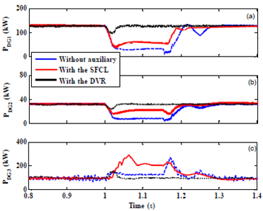
Fig. 5. Operation characteristics of the three DG units under the short-circuit fault. (a) DG1, (b) DG 2 and (c) DG3.

CONCLUSION
Based on the theoretical analysis, simulation study, and economic evaluation, this paper carries out the comparison of the SFCL and the DVR for enhancing the micro-grid’s LVRT capability, and the following conclusions can be obtained. 1) The SFCL and the DVR can both assist the micro-grid to meet the LVRT requirements. 2) Regardless of the full-compensation or non-full-compensation DVR, its total cost is more than the SFCL. Although the full-compensation DVR is able to offer better transient performance indexes, there may be a tradeoff between performance contribution and device cost. 3) Applying the SFCL enables the energy storage unit to offer better control effects in power stabilization. From technical and economic perspectives, the SFCL will be a more preferable choice than the DVR. In the near future, the detailed optimization design and experimental test of the SFCL will be conducted, and the results will be reported later.


REFERENCES
[1]   Baoquan Liu, Fang Zhuo, Yixin Zhu, and Hao Yi, “System Operation and Energy Management of a Renewable Energy-Based DC Micro-Grid for High Penetration Depth Application,” IEEE Trans. Smart Grid, vol. 6, no. 3, pp. 1147–1155, May 2015.
[2]   Feng Zheng, et al., “Transient Performance Improvement of Microgrid by a Resistive Superconducting Fault Current Limiter,” IEEE Trans. Appl. Supercond., vol. 25, no. 3, June 2015, Art. No. 5602305.
[3]   Zhangjie Fu, Sun Xingming, Qi Liu, et al. “Achieving efficient cloud search services: Multi-keyword ranked search over encrypted cloud data supporting parallel computing,” IEICE Trans. Commun., vol. 98, no. 1, pp. 190–200, January 2015.
[4]   Tinghuai Ma, Jinjuan Zhou, Meili Tang, et al. “Social network and tag sources based augmenting collaborative recommender system,” IEICE Trans. Inf. Syst., vol. 98, no. 4, pp. 902–910, April 2015.
[5]   Zhihua Xia, Xinhui Wang, Xingming Sun, et al. “A Secure and Dynamic Multi-Keyword Ranked Search Scheme over Encrypted Cloud Data,” IEEE Trans. Parallel Distr. Syst., vol. 27, no. 2, pp. 340–352, Feb. 2016

Sunday 26 August 2018

Cascaded Open-End Winding Transformer based DVR

2016, IEEE

ABSTRACT
This paper introduces and generalizes a class of multilevel dynamic voltage restorer (DVR) for voltage sags/swells compensation of high-power sensitive loads. Such a device can improve the power quality of sensitive loads located in stiff systems. The proposed DVR is based on three-phase bridge converters series-connected by means of cascaded transformers using the concept of open-end winding (OEW). Hence, two DC links can provide either symmetrical (i.e., equal DC-link voltages) or asymmetrical (i.e., different DC-link voltages) operation of the DVR converters. Generalization for K-stages is presented as well. The proposed configuration is named as DVR-COEW (i.e., cascaded open-end winding). Such a topology permits to generate a maximized number of voltage levels per converter leg. The multilevel waveforms at the output voltages of the converter are generated by using a suitable PWM strategy associated with both: i) DC-link voltages ratio and ii) transformers turns ratio. Modularity and simple maintenance make the proposed DVRCOEW an attractive solution compared to some conventional configurations. The model and PWM control are addressed in this paper. Simulation and experimental results are presented.

KEYWORDS:
  1. Dynamic voltage restorer (DVR)
  2. Open-end winding (OEW)
  3. DC-link voltages
  4. Pulse Width Modulation (PWM)

SOFTWARE: MATLAB/SIMULINK

BLOCK DIAGRAM:

Fig. 1. Example of a DVR-based system

EXPECTED SIMULATION RESULTS:
Figure 2. Phase-voltage of the resultant converter in phase-(vra) for conventional and proposed DVRs considering an operation with 1-stage (i.e.,= 1 with N1 = 1) having converters with a total of 6 legs. (a) Conventional DVR. (b) Proposed COEW-DVR and symmetrical DC-link voltages (i.e., DC link voltage ratio 1:1). (c) Proposed COEW-DVR and asymmetrical DC-link voltages (i.e., DC-link voltages ratio 2.:1)
Fig. 3. Figure 7. Phase-voltage of the resultant converter in phase-(vra) for conventional and proposed DVRs considering an operation with 2-stages (i.e., = 2) having converters with a total of 12 legs. (a) Conventional DVR with N1 = 1 and N2 = 3. (b) Proposed COEW-DVR and asymmetrical DC-link voltages (i.e., DC-link voltage ratio 2:1) N1 = 1 and N2 = 2. (c) Proposed COEW-DVR and asymmetrical DC-link voltages (i.e., DC-link voltages ratio 4:1) N1 = 1 and N2 = 2.

CONCLUSION
This paper has presented a cascaded open-end winding (COEW) transformer based DVR. The COEW-DVR configuration is generalized for k-stages. A comparison between the proposed and conventional (using HB [6]) configurations (operating with 1-stage) is summarized in Table IV. It can be seen that the proposed COEW-DVR has a better quality of output voltages when compared to the conventional one with HB [6]. This is observed by means of WTHD of the output resultant voltages vrj of the COEW-converter. Additionally, the lower values of WTHD at the output voltages permits the proposed COEW-DVR to reduce its switching frequency to match the same harmonic distortion value obtained for the conventional one. In this way, semiconductor losses would give a fair comparison. The semiconductor losses estimation was done by using the thermal module of PSIM, in which both configurations have operated under the same vrj magnitude and WTHD value. The power of the three-phase load was 6 kW. The conditions and more details for these comparisons under 1-stage operation are found in [19]. Hence, the semiconductor losses estimation for COEW-DVR with 1-stage operation are reduced up to 48.1% compared to the values obtained with conventional one. The losses comparison for 2 stages operation has been done as well. In that case, for the same switching frequency (i.e., fsw =10kHz) the proposed COEW-DVR has presented a reduction of 25% compared to losses obtained for conventional one.

REFERENCES
  • Koval and M. Hughes, “Canadian national power quality survey: frequency of industrial and commercial voltage sags,” Industry Applications, IEEE Transactions on, vol. 33, pp. 622–627, May 1997.
  • Affolter and B. Connell, “Experience with a dynamic voltage restorer for a critical manufacturing facility,” in Transmission and Distribution Conference and Exposition, 2003 IEEE PES, vol. 3, pp. 937–939 vol.3, Sept 2003.
  • Lee, G. Venkataramanan, and T. M. Jahns, “Modeling effects of voltage unbalances in industrial distribution systems with adjustablespeed drives,” IEEE Transactions on Industry Applications, vol. 44, pp. 1322–1332, Sept 2008.
  • -m. Ho and H.-H. Chung, “Implementation and performance evaluation of a fast dynamic control scheme for capacitor-supported interline DVR,” Power Electronics, IEEE Transactions on, vol. 25, no. 8, pp. 1975–1988, 2010.
  • W. Li, P. C. Loh, F. Blaabjerg, and D. Vilathgamuwa, “Investigation and improvement of transient response of dvr at medium voltage level,” Industry Applications, IEEE Transactions on, vol. 43, pp. 1309–1319, Sept 2007.

An Improved Direct AC-AC Converter for Voltage Sag Mitigation


 IEEE Transactions on Industrial Electronics, 2013

ABSTRACT
Dynamic Voltage Restorer (DVR) is a definitive solution towards compensation of voltage sag with phase jump. Conventional DVR topologies however have dc-link and two stage power conversion. This increases its size, cost and associated losses. Therefore topologies without the dc-link, mitigating sag by utilizing direct ac-ac converters, are preferable over the conventional ones. As no storage device is employed, compensation by these topologies is limited only by the voltages at the point of common coupling that is feeding the converters. In this paper, a direct ac-ac converter based topology fed with line voltages is proposed. The arrangement provides increased range of compensation in terms of magnitude and phase angle correction. Detailed simulations have been carried out in MATLAB to compare the capability of the proposed topology with other similar topologies.

KEYWORDS:
1.      Dynamic voltage restorer (DVR)
2.      Voltage source inverter (VSI)
3.      Voltage sag compensation
4.      Voltage phase jump compensation.
5.      AC-AC converter

SOFTWARE: MATLAB/SIMULINK

BLOCK DIAGRAM:

Fig. 1. Interphase ac-ac converter topology


Fig. 2. Proposed converter topology.

EXPECTED SIMULATION RESULTS:

Fig. 3. Compensation of a sag type Ba. (a) Three phase voltage at the PCC with sag of 0.3 p.u. magnitude and 􀀀100 phase jump. (b) Three phase load voltage(c) Injected voltage. (d) The duty cycle of choppers in phase a sag supporter.


Fig. 4. Compensation of a sag type Ca. (a) Three phase voltage at the PCC with sag of 0.4 p.u. characteristic voltage magnitude and 􀀀200 phase jump. (b) Three phase load voltage at the PCC. (c) Injected voltages. (d) The duty cycle of voltages in phase b sag supporter. (e) The duty cycle of choppers in phase c sag supporter.

Fig. 5. Compensation  of  symmetrical  sag. (a) Three phase voltage at the PCC with sag of 0.5 p.u. magnitude and 􀀀600 phase jump. (b) Three phase load voltage at the PCC. (c) Injected voltages. (d) The duty cycle of voltages
in all sag supporters.

CONCLUSION
In this paper, an ac-ac converter based voltage sag supporter fed with line voltage has been proposed to compensate voltage sag with phase jump. The operation and switching logic of this topology are explained in detail. The capability of the topology is tested for different types of voltage sags are compared with other topologies. This topology has the advantage of eliminating storage device and providing increased range of compensation. The efficacy of the proposed topology is validated through simulation and experimental studies. An intuitive method of classification of voltage sags [2], assorts sag into four basic types as shown in Fig. In the figure, the dashed lines represent the pre-sag voltage, and the solid lines represent the voltages during sag. The pre-sag voltages are given by V j , and during sag voltages by V0 j ,where j = a, b, and c. A single phase fault causes voltage sag in one phase (type B) at the terminals of a star connected load and in two phases (type C) at the terminals of a delta connected load. A phase-to-phase fault causes type C sag at the terminals of a star connected load and type D sag at the terminals of a delta connected load. A three phase symmetrical sag (type A) is caused by three phase fault. Further, voltage sag gets transformed into other sag types as it propagates in power system to lower voltage levels through transformers. Transformation of a voltage sag due to single phase fault i.e. type B sag, is illustrated in Fig. The type B sag when propagates through a star-delta transformer it transforms to a type C sag. When type C sag in-turn propagates through a star-delta transformer, it transforms to a type D sag. Each sag type is further classified into three subtypes based on the phase(s) that is/are affected. The subtypes are represented by a, b or c subscript, for easy reference. For instance, sag type Ba and Da have voltage sag in phase-a; while for sag type Ca, the line voltage bc is faulty and phase- a is healthy. Characterization of each type of sag is done in terms of the type and the complex characteristic voltage (V0 ch). The characteristic voltage defines three phase voltage sag. The phase voltages as a function of the characteristic voltage and the pre-fault voltage (which is usually 1 p.u.) is given in Table IV for the basic four types [2].

REFERENCES
[1]         R. S. Vedam and M. S. Sarma, Power Quality: VAR Compensation in Power Systems. CRC press, 2009.
[2]         M. H. J. Bollen, Understanding Power Quality Problems. New York: IEEE press, 2000.
[3]         M. Mohseni, S. M. Islam, and M. A. Masoum, “Impacts of symmetrical and asymmetrical voltage sags on dfig-based wind turbines considering phase-angle jump, voltage recovery, and sag parameters,” IEEE Trans. Power Electron., vol. 26, no. 5, pp. 1587–1598, May 2011.
[4]         A. Massoud, S. Ahmed, P. Enjeti, and B. Williams, “Evaluation of a multilevel cascaded-type dynamic voltage restorer employing discontinuous space vector modulation,” IEEE Trans. Ind. Electron., vol. 57, no. 7, pp. 2398–2410, Jul. 2010.
[5]         Y. W. Li, D. Vilathgamuwa, F. Blaabjerg, and P. C. Loh, “A robust control scheme for medium-voltage-level dvr implementation,” IEEE Trans. Ind. Electron., vol. 54, no. 4, pp. 2249–2261, Aug. 2007.