asokatechnologies@gmail.com 09347143789/09949240245

Search This Blog

Wednesday, 12 June 2019

Hybrid Modulation Concept for Five-Level Active-Neutral-Point-Clamped Converter


 ABSTRACT:  
In this letter, a hybrid modulation concept consisting of three-level space vector modulation (3L-SVM) and phase-shifted pulse width modulation (PS-PWM) is proposed for five-level active neutral- point-clamped (5L-ANPC) converter. Under this concept, a simpler 3L-SVM plus PS-PWM scheme is applied to realize 5L modulation, instead of using complex 5L-SVM. The control of neutral voltage, flying capacitor voltage, and the improved dc voltage utilization are all implemented. With the help of the proposed concept,   well-developed 3L-SVM schemes can be directly applied to the 5L-ANPC converter, which significantly simplify the gating signal generation. This concept can also be applied to other hybrid clamped 5L converters with two dc-link capacitors. It provides a unique solution, which utilize lower level SVM scheme to control higher level multilevel converters.

KEYWORDS:
1.      Five-level active-neutral-point-clamped (5LANPC)
2.      Multilevel converter
3.      Phase-shifted pulse width modulation (PS-PWM)
4.      Space vector modulation (SVM)

SOFTWARE: MATLAB/SIMULINK

CIRCUIT DIAGRAM:


Fig. 1 Single-phase circuit of a 5L-ANPC converter.

 EXPECTED SIMULATION RESULTS:


Fig. 2. Waveforms of modulation wave Vma , phase voltage vphase , line–line voltage vl l , three-phase current, two dc-link capacitor voltage, and three-phase FC voltage of 5L-ANPC converter with proposed hybrid modulation concept: (a) M = 0.23. (b) M = 1.15. (c) Neutral voltage and FC voltage control.


Fig. 3. Comparison waveforms of modulation wave Vma , phase voltage vphase , line–line voltage vl l , three-phase current, two dc-link capacitor voltage, and three-phase FC voltage of 5L-ANPC converter with PS-PWM in [5]: (a) M = 0.23. (b) M = 1.15. (c) Neutral voltage and FC voltage control.

CONCLUSION:

In this letter, a new hybrid modulation concept is proposed for 5L-ANPC converters. Instead of using 5L-SVM, it applies 3L-SVM plus PS-PWM to modulate the 5L-ANPC converters. With the proposed concept, the control of neutral voltage, FC voltage, and the increased voltage utilization are all realized.  Well-developed 3L-SVM schemes can be applied directly to simplify the modulation process. The simulation and experiment have proved the effectiveness of the modulation scheme. Although this modulation concept is developed for 5L-ANPC converter, it can also be applied to other hybrid 5L converters with two dc-link capacitors [13]. By dividing these converters into two cells, 3L-SWM can be applied to their 3L converter cells, while both cells are together modulated by PS-PWM using the modulation waves derived from 3L-SVM. The proposed concept provides a unique solution which utilize lower level SVM scheme to modulation higher level multilevel converters at desired performance.
REFERENCES:
[1] S. Kouro, J. Rodriguez, B. Wu, S. Bernet, and M. Perez, “Powering the future of industry: High-power adjustable speed drive topologies,” IEEE Ind. Appl. Mag., vol. 18, no. 4, pp. 26–39, Jul./Aug. 2012.
[2] P. Barbosa, P. Steimer, J. Steinke, M. Winkelnkemper, and N. Celanovic, “Active-neutral-point-clamped (ANPC) multilevel converter technology,” in Proc. Power Electron. Appl. Eur. Conf., 2005, pp. 1–10.
[3] J. Li, Z. Pan, and R. Burgos, “A new control scheme of five-level active NPC converters for common mode voltage mitigation in medium voltage drives,” in Proc. IEEE Energy Convers. Congr. Expo., 2014, pp. 234–241.
[4] R. T. Hamid, S. Danny, M. M. Kashem, and C. Phil, “Novel modulation  and control strategy for five-level ANPC converter with unbalanced DC voltage applied to a single-phase grid connected PV system,” in Proc.  IEEE Ind. Appl. Soc. Annu. Meet., 2013, pp. 1–8.
[5] K. Wang, L. Xu, Z. Zheng, and Y. Li, “Capacitor voltage balancing of a five-level ANPC converter using phase-shifted PWM,” IEEE Trans. Power  Electron., vol. 30, no. 3, pp. 1147–1156, Mar. 2015.

A Novel Modulation Technique and a New Balancing Control Strategy for a Single-Phase Five-Level ANPC Converter


 ABSTRACT:  
This paper proposes a novel modulation technique and a new balancing control strategy for a single-phase five-level flying-capacitor (FC)-based active-neutral-point-clamped (ANPC) converter. The proposed modulator can control the FC voltage to follow the requested reference value and simultaneously generate the required ac output voltage regardless of the values of the dc capacitor voltages of the converter. By implementing this method, smaller values of the dc-link capacitor and FC can be used even in applications that could experience ripple or transient in the capacitor voltage. In a single-phase five-level ANPC converter applications, where the capacitors can experience pulsation power and dc-link balancing issues, such as grid-connected photovoltaic system, the selection of the reference voltage value for the FC can play an important role to balance the average values of the dc-link  capacitor voltage. The proposed new control strategy uses a new reference voltage for the FC to be applied by the new modulator to have an average balanced dc-link voltages as well as an ac output voltage with good power quality. Simulation studies and experimental results demonstrate the effectiveness of the proposed modulation technique and control strategy even with relatively small dc capacitors to produce high-quality output voltage and current waveforms while maintaining an average balanced dc-link voltages.
KEYWORDS:
1.      Active-neutral-point-clamped (ANPC) converter
2.      Flying capacitor (FC)
3.       Multilevel converters
4.      Photovoltaic (PV) power system
5.      Pulse width modulation
6.      Voltage balancing
SOFTWARE: MATLAB/SIMULINK
CIRCUIT DIAGRAM:


Fig. 1. Single-phase 5L-ANPC converter.

 EXPECTED SIMULATION RESULTS:


Fig. 2. Results of applying conventional modulation technique with dc-link capacitors equal to 300 μF. (a) DC-link voltage, dc-link capacitor voltages, and FC voltage. (b) Inverter output voltage. (c) Inverter output and ac grid current. (d) Magnitude of current harmonics (p.u.).


Fig. 3. Results of applying conventional modulation technique with dc-link
capacitors equal to 3 mF. (a) DC-link voltage, DC-link capacitor voltages, and
FC voltage. (b) Inverter output voltage. (c) Inverter output and ac grid current.
(d) Magnitude of current harmonics (p.u.).


Fig. 4. Results of applying proposed modulation technique with dc-link
capacitors equal to 300 μF and FC reference voltage equal to Vdc/4. (a) DClink
voltage, dc-link capacitor voltages, and FC voltage. (b) Inverter output
voltage. (c) Inverter output and ac grid current. (d) Magnitude of current
harmonics (p.u.).


Fig. 5. Results of applying proposed modulation technique with dc-link
capacitors equal to 300 μF and FC reference voltage equal to half of the engaged
dc-link capacitor in each output half-cycle. (a) DC-link voltage, dc-link
capacitors voltages, and FC voltage. (b) Inverter output voltage. (c) Inverter
output and ac grid current. (d) Magnitude of current harmonics (p.u.).


Fig. 6. Results of applying the proposed modulation technique with the proposed
FC reference voltage with having step power in the PV and transmission
power to the grid at t = 37 ms: (a) DC-link voltage, dc-link capacitors voltage,
and FC voltage. (b) Inverter output and grid current.

CONCLUSION:

A novel modulation and control strategy for a five-level FC based ANPC converter has been presented. A theoretical framework of a novel extended modulation technique for unsymmetrical and symmetrical voltage conditions of a 5L-ANPC converter has been proposed. The application of the proposed modulation and control strategy, for a single phase grid-connected PV system using a five-level FC-based ANPC converter to produce ac output voltages with good power quality under both symmetrical and unsymmetrical conditions, has been investigated. Issues related to the balancing of dc-link voltages and its associated problems are discussed, and a new control strategy has been introduced to solve the dc-link voltage divergence problem. The proposed strategy is applicable for other applications of the five-level FC-based ANPC converter.  The effectiveness of the proposed modulation technique and control strategy was demonstrated by the simulation and experimental results in the laboratory, demonstrating the ability of the system to operate properly using smaller size dc-link capacitors to produce ac output voltage and current waveforms with good power quality while maintaining dc-link average voltage balancing.
REFERENCES:
[1] J. I. Leon, L. G. Franquelo, S. Kouro, B. Wu, and S. Vazquez, “Simple modulator with voltage balancing control for the hybrid five-level flying-capacitor based ANPC converter,” in Proc. IEEE ISIE, 2011, pp. 1887–1892.
[2] P. Barbosa et al., “Active neutral-point-clamped multilevel converters,” in Proc. 36th IEEE PESC, 2005, pp. 2296–2301.
[3] F. Kieferndorf et al., “ANPC-5L technology applied to medium voltage variable speed drives applications,” in Proc. Int. SPEEDAM, 2010, pp. 1718–1725.
[4] S. A. Gonzalez, M. I. Valla, and C. F. Christiansen, “Five-level cascade asymmetric multilevel converter,” IET Power Electron., vol. 3, no. 1,   pp. 120–128, Jan. 2010.
[5] Y. Kashihara and J. Itoh, “Parameter design of a five-level inverter for PV systems,” in Proc. 8th IEEE ICPE ECCE, 2011, pp. 1886–1893.

A Carrier-Based PWM Strategy With the Offset Voltage Injection for Single-Phase Three-Level Neutral-Point-Clamped Converters


ABSTRACT:  
Single-phase three-level neutral point clamped (NPC) converters are widely applied in high-speed railway electrical traction drive systems.  A significant problem related to the single-phase three-level NPC converters is the fluctuation of the neutral-point voltage. In this paper, a capacitor voltage balancing technique is proposed that injects an offset voltage into the sinusoidal modulating signals of the conventional carrier-based pulse width modulation (CBPWM) method. Furthermore, when the injected offset voltage is maximized, it cannot only balance the dc-link capacitors voltages, but also reduce switching losses. Theoretical analysis has shown that both methods can control the neutral point voltage effectively, but the neutral point voltage controller in the CBPWM with maximum offset voltage injection (CBPWM-MOVI) has a faster dynamic response. It was observed that the high-order harmonics frequencies of the line current are centered around the twice switching frequency in the CBPWM with the offset voltage injection (CBPWM-OVI) but are centered around the switching frequency in the CBPWM-MOVI. And also, the CBPWM-MOVI has switching commutations number at least 25% below that of the CBPWM-OVI in one modulating signal period. The performances of the two strategies were verified by simulation and experimental tests.
KEYWORDS:
1.      Carrier-based pulse width modulation (CBPWM),
2.      Neutral-point voltage balancing
3.      Single-phase
4.      The offset voltage injection
5.      Three-level converter
SOFTWARE: MATLAB/SIMULINK
CIRCUIT DIAGRAM:


Fig. 1. Single-phase three-level NPC converter.

 EXPECTED SIMULATION RESULTS:


Fig. 2. Simulation results of the main voltage us and the line current is .
(a) CBPWM-OVI with k = 0.5. (b) CBPWM-MOVI.


Fig. 3. Simulation results of FFT analysis for frequency spectrum of the line
current is . (a) CBPWM-OVI with k = 0.5. (b) CBPWM-MOVI.


Fig. 4. Simulation results of the input port voltage uab . (a) CBPWM-OVI
with k = 0.5. (b) CBPWM-MOVI.


Fig. 5. Simulation results of dc-link voltage u1 and u2 . (a) CBPWM-OVI
with k = 0.5. (b) CBPWM-MOVI.


Fig. 6. Simulation results of dc-link voltage error, the modulating signal
and the offset voltage. (A) CBPWM-OVI with k = 0.5. (B) CBPWM-MOVI.
(C) CBPWM-MOVI (partial enlarged view).

CONCLUSION:

This paper proposes CBPWM strategies in conjunction with an offset voltage injection for a single-phase three-level NPC converter to achieve neutral point voltage control and PWM drive signals generation. The restriction range of the offset voltage is discussed in details. Based on this, this paper presents a CBPWM strategy with the maximum offset voltage injection. The salient features of the proposed CBPWM-OVI and CBPWM-MOVI strategies are as follows:
1) both methods guarantee to achieve voltage balancing, while the CBPWM-MOVI has a faster dynamic response of the neutral point voltage controller than the CBPWMOVI;
2) the high-order harmonics of the line current distribute around at twice switching frequency 2fs in the CBPWMOVI, and the same as the switching frequency in the CBPWM-MOVI;
3) the total number of switching commutations of CBPWMMOVI is 25% below that of the CBPWM-OVI, at least in a modulating signal period;
4) both CBPWM-OVI and CBPWM-MOVI with voltage step compensation can guarantee the maximum voltage level step to be half of the dc-link voltage compared with the existing CBPWM strategy.
Simulation and experimental results verify the validity and feasibility of these conclusions, and the proposed CBWMOVI and CBPWM-MOVI strategies are also desirable for single-phase three-level NPC UPS inverter or solar inverter applications.
REFERENCES:
[1] R. Hill, “Electric railway traction—Part II. Traction drives with three phase induction motors,” Power Eng. J., vol. 8, no. 3, pp. 143–152, Jun. 1994.
[2] A. Steimel, “Electrical railway traction in Europe,” IEEE Ind. Appl.Mag., vol. 2, no. 6, pp. 6–17, Nov./Dec. 1996.
[3] A. Cheok, S. Kawamoto, T.Matsumoto, and H. Obi, “High power AC/DC converter and DC/AC inverter for high speed train applications,” in Proc. TENCON Conf., 2000, pp. 423–428.
[4] A. Nabae, I. Takahashi, and H. Akagi, “A new neutral-point-clamped PWM inverter,” IEEE Trans. Indus. Appl., vol. IA-17, no. 5, pp. 518– 523, Sep. 1981.
[5] J. Lai and F. Peng, “Multilevel converters—A new breed of power converters,” IEEE Trans. Ind. Appl., vol. 32, no. 3, pp. 509–517, May/Jun. 1996.

Sunday, 9 June 2019

Novel Single Stage Power Factor Corrected LED Driver Topology for Space Constrained Applications of Aircraft Exterior Lighting System


ABSTRACT:
This paper proposes a novel converter topology based on a single stage LED driver with Power Factor  Correction (PFC) which is optimized for weight, volume and cost, for space constrained environments such as Aerospace exterior lighting product. The proposed topology utilizes a single switch to harmonize the input current as well as control the intensity of lighting system.
A typical Power Factor Pre-regulator (PFP) uses a bulk energy storage capacitor, which is subjected to wear out at higher altitudes due to low pressure conditions and freezes at  negative temperatures, resulting in poor reliability converter for Aerospace applications. Unlike a regular Power Factor Pre-regulator (PFP), the proposed topology avoids the use of bulk energy storage capacitor which results in a fast transient response with enhanced reliability, reduced board real estate and weight. The proposed LED driver topology can control the LED current with both Buck and Boost mode of control, making it a good choice for applications with wide input voltage variation.
A 110 W prototype based on proposed converter was built to verify the operation of proposed topology. The experimental results are in line with the predicted performance. The proposed converter is able to achieve a power factor of 0.988 with an input current THD of < 10%.

SOFTWARE: MATLAB/SIMULINK

 BLOCK DIAGRAM:


Figure 1. Proposed LED driver topology with single stage active PFC

 EXPECTED SIMULATION RESULTS:


Figure 2. Measured waveforms at 90V AC input (a) Input Voltage (Red) (b) Input current (Blue) (c) Average Voltage drop across LED current sense resistor (green) (Equivalent to LED average current as the sense resistor value is 1ohm.


Figure 3. Measured Linear FFT of input current
 

Figure 4. Start-up transient at 90V AC input (a) Input Voltage (Red) (b) Input current (Blue) (c) Average Voltage drop across LED current sense resistor (Green)(Equivalent to LED average current as the sense resistor value is 1ohm.


Figure 5. Current profiles through various power circuit components (a) LED Current (Green) (b) Current through MOSFET M1 (Red) (c) Current through inductor L2 (Blue) (d) Current through Inductor L1 (Purple)


Figure 6. Current profiles through various power circuit components (a) LED Current (Green) (b) Current through MOSFET M1 (Red) (c) Current through inductor L2 (Blue) (d) Current through Inductor L1 (Purple)


Figure 7. Measured waveforms at 132V AC input (a) Input Voltage (Light Blue) (b) Input current (Blue) (c) Average Voltage drop across LED current sense resistor (Red).


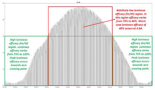
Figure 8. LED current profile over one rectified line cycle

CONCLUSION:
This paper presents a novel LED driver topology, capable of input power factor correction, for space constrained applications, such as Aerospace exterior lighting product line. Due to the compact design of the proposed LED driver topology, it can be of great advantage for an integrated power supply solution for Aerospace exterior lighting product offerings. The proposed LED driver topology can control the LED current with both Buck and Boost mode  of control, making it a good choice for applications with wide input voltage variation. The proposed LED driver topology has been verified by mathematical analysis, circuit simulation and performance has been demonstrated experimentally as well. The proposed LED driver topology promises an appreciable amount of savings in term of real estate, power loss, and heat sink requirements while enhancing the power density of the converter and its  reliability. Typically, it’s the bulk output capacitor that wears out with pressure variation (wear out phenomenon accelerates at altitudes more than 8000m due to the reduced pressures); which can be avoided with the proposed topology. Depending upon the load (number of LEDs) and input voltage; in order to protect LEDs, a reverse blocking diode may be required during the Buck operation. For  Boost application, reverse blocking diode will not be required even with today’s technology. Authors have been granted a U.S. Patent 9363291 [8] against the proposed novel LED driver topology.
 
REFERENCES:
[1] L. H. Dixon, "High Power Factor Preregulators for Off- Line Power Supplies," Unitrode Power Supply Design Seminar Manual SEM600, 1988. (Republished in subsequent Manuals)
[2] Spiazzi, G., and Mattavelli, P. (1994) “Design criteria for power factor preregulators based on SEPIC and Cuk converters in continuous conduction mode,” IEEE IAS Conference Record, 1994, 1084-1089.
[3] Z. Ye, F. Greenfeld, and Z. Liang, “Single-stage offline SEPIC converter with power factor correction to drive high brightness LEDs,” in Proc. IEEE Appl. Power Electron. Conf., 2009, pp. 546–553.
[4] C.Zhou and M.Jovanovic, "Design Trade-offs in Continuous Current-Mode Controlled Boost Power-Factor Correction Circuits", HFPC Cod. Proc., 1992, pp. 209-220
[5] L. H. Dixon, "Average Current Mode Control of  Switching Power Supplies," Unitrode Power Supply Design Seminar Manual SEM700, 1990