asokatechnologies@gmail.com 09347143789/09949240245

Search This Blog

Monday, 18 July 2022

An Adaptive Off-Time Controlled DCM Flyback PFC Converter With Unity Power Factor and High Efficiency

ABSTRACT:

Constant duty cycle controlled discontinuous conduction mode (DCM) flyback power factor correction (PFC) converter has the advantage of high power factor (PF) and the disadvantage of low efficiency. While, constant on-time (COT) controlled critical conduction mode (CRM) flyback PFC converter has the exact opposite features, besides its switching frequency varies in a line cycle, and the variation range is very large, which complicates the electromagnetic interference (EMI) design. In order to obtain both benefits of these two control methods, an adaptive off-time (AOT) control technique for DCM flyback PFC converter is proposed in this paper. By utilizing the output voltage and the amplitude of line voltage to adjust the off-time of the main switch, the magnetizing current of transformer exactly operates in CRM when the rectified input voltage gets the peak. Thus, the root-mean-square (RMS) current of the main switch and the diode, as well as the conduction loss can be effectively reduced, and high efficiency can be obtained. The proposed control technique also can achieve theoretical unity PF over universal input voltage range of 90_264VAC. Moreover, its variation range of switching frequency is greatly reduced compared to that of COT control. A 60W prototype has been fabricated and tested in the laboratory and experimental results are presented to verify the effectiveness of the proposed method.

KEYWORDS:

1.      Adaptive control

2.      Flyback converter

3.      Power factor

SOFTWARE: MATLAB/SIMULINK

 BLOCK DIAGRAM:


Figure 1. Block Diagram And Key Waveforms Of Aot Controlled Dcm Flyback Pfc Converter.

 EXPECTED SIMULATION RESULTS:

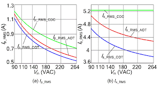
Figure 2. The Rms Current Of The Main Switch And The Diode Of Flyback Pfc Converter With The Aforementioned Three Control Methods For Different Vin.


Figure 3. The Peak Current Of The Main Switch And The Diode Of Flyback Pfc Converter With The Aforementioned Three Control Methods For Different Vin.


Figure 4. Bode Plot Of Aot Control Loop.

CONCLUSION:

This paper proposes an adaptive off-time controlled DCM flyback PFC converter. According to the output voltage and the amplitude of line voltage, the proposed controller adaptively adjusts the off-time of the main switch, so that the magnetizing current of the transformer can exactly operate in CRM. This operation mode can effectively reduce the conduction loss of the main switch and increase efficiency, and on the other hand, similar with constant duty cycle control, the duty cycle and the switch period of AOT control remains fixed during each line cycle, therefore, theoretical unity PF and sinusoidal input current can be also obtained over universal input voltage range. Moreover, the variation range of the switching frequency of AOT control strategy is greatly narrowed compared to that of COT control, which will bring potential convenience in the input filter design. A 60W experimental prototype has been built to verify the theoretical analysis. Experimental results show the minimal PF of AOT control and constant duty cycle control is 0.994, which is significantly higher the minimal PF 0.92 of COT control, and the highest efficiency of AOT control and COT control is 87.6%, which is obviously higher than the highest efficiency 86.5% of constant duty cycle control.

REFERENCES:

[1] M. M. Jovanovic andY. Jang, ``State-of-the-art, single-phase, active power- factor-correction techniques for high-power applications_An overview,'' IEEE Trans. Ind. Electron., vol. 52, no. 3, pp. 701_708, Jun. 2005.

[2] O. Garcia, J. A. Cobos, R. Prieto, P. Alou, and J. Uceda, ``Single phase power factor correction: A survey,'' IEEE Trans. Power Electron., vol. 18, no. 3, pp. 749_755, May 2003.

[3] C. Qiao, G. Feng, and K. M. Smedley, ``A topology survey of single- stage power factor corrector with a boost type input-current-shaper,'' IEEE Trans. Power Electron., vol. 16, no. 3, pp. 360_368, May 2001.

[4] Z. Chen, P. Davari, and H. Wang, ``Single-phase bridgeless PFC topology derivation and performance benchmarking,'' IEEE Trans. Power Electron., vol. 35, no. 9, pp. 9238_9250, Sep. 2020, doi: 10.1109/tpel.2020.2970005.

[5] H. Luo, J. Xu, D. He, and J. Sha, ``Pulse train control strategy for CCM boost PFC converter with improved dynamic response and unity power factor,'' IEEE Trans. Ind. Electron., vol. 67, no. 12, pp. 10377_10387, Dec. 2020.

Advanced PET Control for Voltage Sags Unbalanced Conditions Using Phase-Independent VSC-Rectification

ABSTRACT:

The power electronic transformer (PET) is an emerging technology that is quickly becoming a key component of the next-to-come power distribution networks (PDNs), due to its versatility on energy management, as well as, the improvement on the quality of the energy. PDNs are characterized by their unbalanced conditions, causing that PETs driven by conventional dq0 controls introduce current distortions on the primary winding of the transformer. Such distortion is evidenced in the 2! oscillations of Vd and Vq acting as harmonic sources. In this sense, this paper proposes a novel control approach for PETs. The key idea behind of this proposal consists of operating each phase independently, which is achieved through the enclosed rectification and the mitigation of the 2! Oscillations in a Dual Active Bridge (DAB) topology. The attained advantages by this control scheme are: (a) balancing of the primary winding currents; (b) unitary power factor; (c) negligible harmonic distortion; and (d) 2! oscillation mitigation on the DC bus.

KEYWORDS:

1.      AC-DC-AC

2.      Power conversion

3.      Power electronic transformer

4.      Dual active bridge

5.      VSC

6.      Unbalanced control

7.       Voltage sags

8.      Unbalanced input voltages.

SOFTWARE: MATLAB/SIMULINK

CIRCUIT DIAGRAM:


Fig. 1. Three-phase VSC rectifier with an unbalanced control

EXPECTED SIMULATION RESULTS:


Fig. 2. Simulation for an unbalanced voltage sag during V a g = 1\0_; V b g = 0:5\ 􀀀 120_; V c g = 0:5\120__

.


Fig. 3. Simulation for an unbalanced voltage sag during V a g = 1\0_; V b g = 1\ 􀀀 120_; V c g = 0:1\120__

.


Fig.4. Simulation for an unbalanced voltage sag during V a g = 0:8\0_; V b

g = 0:6\ 􀀀 133:9_; V c g = 0:6\133:9__

.


Fig. 5. Simulation for an unbalanced voltage sag with dq0 control during V a g = 1\0_; V b g = 1\ 􀀀 120_; V c g = 0:1\120__

.

CONCLUSION:

The main contribution of this work consists in a new control structure, which employ a phasorial approach with a single PI control, for PETs working on distribution systems where the operation with unbalanced input voltages is frequently. The capacity of this control of independently generate the modulation variables mabc i with different magnitudes and angles, reach a better performance than other control structures; dq0, for example, to mitigate the problems caused by unbalanced input voltages conditions. Under these input conditions in a PET, the advantages achieve by the proposed control are: (i) balanced AC input currents, (ii) sinusoidal AC input current, and (iii) PF = 1. Furthermore, the control structure is an easy-to-implement and requires no additional components. Finally, in this work, all the advantages mentioned above were validated by using simulation and a lab prototype.

REFERENCES:

[1] H. Chen and D. Divan, “Soft-switching solid-state transformer (s4t),” IEEE Trans. Power Electr., vol. 33, no. 4, pp. 2933–2947, 2018.

[2] H. Chen, A. Prasai, and D. Divan, “Dyna-c: A minimal topology for bidirectional solid-state transformers,” IEEE Trans. Power Electr., vol. 32, no. 2, pp. 995–1005, 2017.

[3] G. Brando, A. Dannier, and A. Del Pizzo, “A simple predictive control technique of power electronic transformers with high dynamic features,” in 5th IET Intern. Conf. on Power Electr., Mach. and Drives, 2010, pp. 1–6.

[4] K. K. Mohapatra and N. Mohan, “Matrix converter fed open-ended power electronic transformer for power system application,” in IEEE PES GM - Conversion and Delivery of Electrical Energy in the 21st Century, 2008, pp. 1–6.

[5] D. Wang, C. Mao, J. Lu, S. Fan, and F. Peng, “Theory and application of distribution electronic power transformer,” Electric Power Syst. Research, vol. 77, no. 3, pp. 219–226, 2007.

Adaptive Power Decoupling Control for Single-Phase Converter with Unbalanced DC-Split-Capacitor Circuit

 ABSTRACT:

This paper proposes an adaptive power decoupling control strategy for a single-phase rectifier with an unbalanced split-capacitor decoupling circuit. Since a capacitance mismatch estimator is integrated into the control strategy, the impact of capacitance mismatch is eliminated. Meanwhile, the capacitance mismatch estimator can provide an auxiliary online monitor for the health of split-capacitors. Moreover, the mechanism of capacitor voltages self-balance is explained. Finally, experiments are conducted to verify the effectiveness of the proposed method.

KEYWORDS:

1.      Active power decoupling

2.       Adaptive control

3.      Dc split- capacitor

4.      Single-phase converter

5.      Capacitance mismatch

SOFTWARE: MATLAB/SIMULINK

SCHEMATIC DIAGRAM:


Fig. 1. Proposed control diagram for single-phase power converter with DC split- capacitor power decoupling circuit.


EXPECTED SIMULATION RESULTS:


Fig. 2. Simulation results of the proposed adaptive decoupling controller. (a) Case I; (b) Case II; (c) Case III.


CONCLUSION:

In this paper, an adaptive power decoupling controller is proposed for the DC split-capacitor decoupling circuit under  capacitance mismatch. The conclusions are listed below: 1) The steady-state analysis of DC split-capacitor decoupling circuits shows that there are infinite feasible solutions to achieve the decoupling of twice ripple power under capacitance mismatch. Among them, a special solution is to control the capacitor voltages into DC and the fundamental frequency sinusoidal AC component. 2) Under the framework of the special solution, an adaptive power decoupling controller is proposed to realize the decoupling of twice ripple power. 3) The capacitance mismatch estimator is presented to estimate the unequal factor online. Consequently, the fundamental frequency power ripple caused by capacitor mismatch is eliminated. Meanwhile, the estimated unequal factor can be used as a health monitoring indicator of split-capacitors.

REFERENCES:

[1] Y. Sun, Y. Liu, M. Su, W. Xiong, and J. Yang, “Review of active power decoupling topologies in single-phase systems,” IEEE Transactions on Power Electronics, vol. 31, no. 7, pp. 4778–4794, Jul. 2016.

[2] H. Hu, S. Harb, N. Kutkut, I. Batarseh, and Z. J. Shen, “A review of power decoupling techniques for microinverters with three different decoupling capacitor locations in PV systems,” IEEE Transactions on Power Electronics, vol. 28, no. 6, pp. 2711–2726, Jun. 2013.

[3] Y. Yang, X. Ruan, L. Zhang, J. He, and Z. Ye, “Feed-forward scheme for an electrolytic capacitor-less AC/DC LED driver to reduce output current ripple,” IEEE Transactions on Power Electronics, vol. 29, no. 10, pp. 5508–5517, Oct. 2014.

[4] H. Li, K. Zhang, and H. Zhao, “Dc-link active power filter for highpower single-phase pwm converters,” J. Power Electron., vol. 12, no. 3, pp. 458–467, May 2012.

[5] R. Wang, F. Wang, D. Boroyevich, R. Burgos, R. Lai, P. Ning, and K. Rajashekara, “A high power density single-phase pwm rectifier with active ripple energy storage,” IEEE Transactions on Power Electronics, vol. 26, no. 5, pp. 1430–1443, May 2010.

A Single-Carrier-Based Pulse-Width Modulation Template for Cascaded H-Bridge Multilevel Inverters

ABSTRACT:

Multiplicity of the triangular carrier signals is a criterion for the extension of sinusoidal pulse width modulation, SPWM, to a number of output voltage levels per phase-leg in cascaded H-bridge (CHB) multilevel inverter (MLI). Considering medium and high voltage applications where appreciable number of output voltage levels from CHB MLI is needed, commensurate high number of carrier signals in either classical level- or phase-shifted SPWM scheme for this inverter is inevitable. High-quality output waveforms from CHB MLI system demands precise synchronization of these multi-carrier signals. Sampling issues, memory constraints and computational delays pose difficulties in achieving this synchronization for real-time digital implementation. This study presents a PWM template for CHB MLI. The developed control concept generates adequate modulation templates for CHB inverter wherein a sinusoidal modulating waveform is modified to fit in a single triangular carrier signal range. These templates can be used on CHB inverter of any level with no further control modification. Nearly even distribution of switching pulses, equal sharing of the overall real power among the constituting power switches and enhanced output voltage quality were achieved with the proposed modulation. For a 3-phase, 7-level CHB, simulation and experimental results, for an R-L load, were presented.

KEYWORDS:

1.      Cascaded H-bridge inverter

2.      Sinusoidal pulse-width modulation

3.      Total harmonic distortion

SOFTWARE: MATLAB/SIMULINK

BLOCK DIAGRAM:


Figure 1. Per Phase Block Diagram Of The Multilevel Waveform Template, Mwt, Generation.

EXPECTED SIMULATION RESULTS:


Figure 2. Simulated Output Voltage And Current Waveforms Of The 7-Level Chb Mli With The Proposed Pwm Scheme. (A) Phase A Individual H-Bridge Output Voltages, (B) Phase-Leg Voltages, (C) Line Voltages, (D) Line Currents.


Figure 3. Simulated Dc-Link Voltages, Fft Analyses Of The Phase-Leg And Line Voltage Waveforms And Real Output Power Waveforms. (A) Dc-Link Voltages For The Whole Phases, (B) Fft Analysis Of The Phase-Leg Voltage Waveform From Ipd, Ps And Proposed Modulation Schemes, (C) Fft Analysis Of The Line Voltage Waveform From Ipd, Ps And Proposed Modulation Schemes, (D) Real Output Power Waveforms Of The Individual H-Bridges With The Proposed Spwm Scheme.


Figure 4. Inverter Conduction And Switching Losses For Modulation Index Range Of 0.6 To 1.

 CONCLUSION:

Presented in this paper is a hybridized single carrier-based pulse width modulation scheme for cascaded H-bridge multilevel inverter. Its operational concept wherein a sinusoidal modulating waveform is modified to fit in a single triangular carrier signal range in order to generate the desired output waveform template for the MLI has been explained in detail. The principle of generating the modulating templates is a furtherance of earlier established modulation approaches for multilevel inverters. It has been shown that the generation of the modulating templates is a clear demonstration of the extension of the well-known bipolar PWM to multi-cascaded H-bridge units. Once the templates are generated, it can be used on CHB inverter of any level with no further control modification; only the parameter N need to be specified. From industrial point of view, the presented concept of MWT will find its application in large number of cascaded H-bridge systems because with the proposed modulation, the inverter control system becomes insensitive to the traditional concept of multiplicity of carrier waves as the number of inverter level increases. This will be highly advantageous since the extra control effort of carrier synchronization will be by-passed in the control algorithm. The proposed SPWM ensures nearly even distribution of switching pulses among the constituting power switches using a reverse-voltage-sorting comparison algorithm. Consequently, the real power variations in the entire cascaded H-bridges are kept within a very narrow band. From our findings, the proposed control approach results in a hybrid modulation scheme that mediates between the phase and level-shifted carrier-based SPWM techniques; thereby inheriting the good features in these two modulation schemes. The performance of the proposed SPWM scheme has been presented through scaled down simulations and experiments on a 3-phase, 7-level CHB inverter; results have been adequately presented.

REFERENCES:

1] S. K. Chattopadhyay and C. Chakraborty, ``Full-bridge converter with naturally balanced modular cascaded H-bridge waveshapers for offshore HVDC transmission,'' IEEE Trans. Sustain. Energy, vol. 11, no. 1, pp. 271_281, Jan. 2020, doi: 10.1109/TSTE.2018.2890575.

[2] X. Zeng, D. Gong, M. Wei, and J. Xie, ``Research on novel hybrid multilevel inverter with cascaded H-bridges at alternating current side for high voltage direct current transmission,'' IET Power Electron., vol. 11, no. 12, pp. 1914_1925, Oct. 2018, doi: 10.1049/iet-pel.2017.0925.

[3] R. K. Varma and E. M. Siavashi, ``PV-STATCOM: A new smart inverter for voltage control in distribution systems,'' IEEE Trans. Sus- tain. Energ., vol. 9, no. 4, pp. 1681_1691, Oct. 2018, doi: 10.1109/ TSTE.2018.2808601.

[4] P. Sotoodeh and R. D. Miller, ``Design and implementation of an 11- level inverter with FACTS capability for distributed energy systems,'' IEEE J. Emerg. Sel. Topics Power Electron., vol. 2, no. 1, pp. 87_96, Mar. 2014, doi: 10.1109/JESTPE.2013.2293311.

[5] A. Ahmed, M. S. Manoharan, and J.-H. Park, ``An ef_cient single-sourced asymmetrical cascaded multilevel inverter with reduced leakage current suitable for single-stage PV systems,'' IEEE Trans. Energy Convers., vol. 34, no. 1, pp. 211_220, Mar. 2019, doi: 10.1109/TEC.2018.2874076.

A Single Phase, Single Stage AC-DC Multilevel LLC Resonant Converter With Power Factor Correction

ABSTRACT:

Single stage LLC resonant converters with inherent power factor correction are getting popularity in AC-DC converters due to its reduced size and weight. However, single stage topologies are usually less efficient in regulating the dc bus capacitor voltage pertaining to line and load transients. This paper proposes a multi-level flying capacitor based single stage AC-DC LLC topology to address the issue of voltage balancing of dc-bus capacitor and to reduce the voltage stress of the switching devices. The proposed three-level inverter topology guarantees zero voltage switching, less circulating currents, reduced switching stress and losses. The converter uses bridgeless rectification scheme for better efficiency and the power factor is made nearly unity by operating the source-side inductor in discontinuous current conduction. Variable switching frequency control is used to regulate the output voltage of the converter and pulse width modulation is used to control the dc-bus voltage. This dual control scheme is very effective to keep the dc-bus voltage nearly constant over a wide range of line and load variations. The proposed topology and control scheme have been validated by hardware results on a 250W resistive load.

KEYWORDS:

1.      LLC resonant converters

2.      AC-DC converters

3.      soft switching

4.       PFC

5.      THD

6.      DC bus

SOFTWARE: MATLAB/SIMULINK

BLOCK DIAGRAM:


Figure 1. Proposed Three-Level Single Stage Llc Converter.


EXPECTED SIMULATION RESULTS:


Figure 2. Source Voltage And Current Waveform.


Figure 3. Input Current Waveform Through Input Inductor.


Figure 4. Flying Capacitor Voltage Waveform, Vc1.


Figure 5. Dc Bus Voltage Waveform, Vc1 C Vc2.


CONCLUSION:

This paper has proposed a three-level flying capacitor based topology for AC/DC LLC resonant converters. The converter has a bridgeless topology which reduces the number of con- ducting devices. The controller uses a dual control scheme which varies duty ratio and frequency to regulate DC bus and output DC voltages respectively. The converter is designed to operate in discontinuous conduction mode to obtain a near unity power factor without having any active current control techniques. Furthermore, the topology provides low voltage stress, ZVS for all the four switches, and reduces losses. For verification, a 250W, 230V to 48V AC-DC converter proto- type has been designed and implemented. The DC bus voltage is held constant at 750V with a peak overshoot of 3.3% even when the load is reduced by 30% from full load.

REFERENCES:

[1] A. K. Peter and J. Mathew, ``A three-level half-bridge flying capacitor topology for single-stage AC-DC LLC resonant converter,'' in Proc. IEEE Int. Conf. Power Electron., Drives Energy Syst. (PEDES), Dec. 2018,pp. 1_6.

 [2] A. Hillers, D. Christen, and J. Biela, ``Design of a highly efficient bidirectional isolated LLC resonant converter,'' in Proc. 15th Int. Power Electron. Motion Control Conf. (EPE/PEMC), Sep. 2012, pp. DS2b_13.

[3] J.-H. Kim, M.-Y. Kim, C.-O. Yeon, and G.-W. Moon, ``Analysis and design of boost-LLC converter for high power density AC-DC adapter,'' in Proc. IEEE ECCE Asia Downunder, Jun. 2013, pp. 6_11.

[4] Y. Qiu, W. Liu, P. Fang, Y.-F. Liu, and P. C. Sen, ``A mathemati- cal guideline for designing an AC-DC LLC converter with PFC,'' in Proc. IEEE Appl. Power Electron. Conf. Expo. (APEC), Mar. 2018, pp. 2001_2008.

[5] S.-Y. Chen, Z. R. Li, and C.-L. Chen, ``Analysis and design of single-stage AC/DC LLC resonant converter,'' IEEE Trans. Ind. Electron., vol. 59, no. 3, pp. 1538_1544, Mar. 2012.