asokatechnologies@gmail.com 09347143789/09949240245

Search This Blog

Saturday, 24 November 2018

Thermal Stresses Relief Carrier-Based PWM Strategy for Single Phase Multilevel Inverters


 ABSTRACT

 Enhancing power cycling capability of power semiconductor devices is highly demanded in order to increase the long term reliability of multilevel inverters. Ageing of power switches and their cooling systems leads to their accelerated damage due to excess power losses and junction temperatures. Therefore, thermal stresses relief (TSR) is the most effective solution for lifetime extension of power semiconductor devices. This paper presents a new thermal stresses relief carrier-based pulse width modulation (TSRPWM) strategy for extending the lifetime of semiconductor switches in single-phase multilevel inverters. The proposed strategy benefits the inherent redundancy among switching states in multilevel inverters to optimally relieve the thermally stressed device. The proposed algorithm maintains the inverter operation without increased stresses on healthy switches and without reduction of the output power ratings. In addition, the proposed algorithm preserves voltage balance of the DC-link capacitors. The proposed strategy is validated on single phase five level T-type inverter system with considering different locations of thermal stresses detection. Experimental prototype of the selected case study is built to verify the results. Moreover, comparisons with the most featured strategies in literature are given in detail.
KEYWORDS:

1.      Lifetime extension
2.      long term reliability
3.      multilevel inverter
4.      pulse width modulation (PWM)
5.       thermal stresses relief
SOFTWARE: MATLAB/SIMULINK
BLOCK DIAGRAM


Fig. 1. A schematic diagram of PWM controlled full bridge n-level T-type inverter


 .
EXPECTED SIMULATION RESULTS


Fig. 2. Simulation results of the proposed strategy at TSD in SA11 at mi=0.85.


 Fig. 3. Simulation results of the proposed strategy at TSD in SA11 at mi=0.45.


Fig. 4. Simulation results of the proposed TSRPWM strategy at TSD in SA12 and mi=0.85.


CONCLUSION
This paper has proposed a new carrier-based modulation strategy, called TSRPWM, for single phase multilevel inverters. It retains the same benefits as the conventional carrier PWM methods, i.e., a simple and easy implementation, but presents a significantly reduced power losses and thermal stresses of the stressed semiconductor devices. The main idea of the new proposed strategy is adaptively selecting the redundant switching states in each switching cycle, in order to optimize power losses through the thermally-stressed device. Therefore, both of the junction temperature and temperature cycling of the stressed device are reduced by the proposed strategy compared with normal mode operation of the device. The results of simulation and experimental prototypes are conformed and verified the new proposed concept. A generalized implementation of the proposed TSRPWM, to provide thermal stresses relief for any of the components and for any n-level inverters, is also presented. Moreover, the proposed strategy maintains the inverter operation with the same output ratings, and voltage balance over DC-link capacitors. Finally, the performance of the proposed strategy is compared with the prominent strategies in literature, and the distinction of the proposed strategy has become clear.
REFERENCES

[1] Shaoyong Yang, A. Bryant, P. Mawby, Dawei Xiang, Li Ran, and P. Tavner, “An industry-based survey of reliability in power electronic converters,” IEEE Trans. Ind. Appl., vol. 47, no. 3, pp. 1441–1451, May 2011.
[2] S. E. De Leon-Aldaco, H. Calleja, and J. Aguayo Alquicira, “Reliability and mission profiles of photovoltaic systems: a FIDES approach,” IEEE Trans. Power Electron., vol. 30, no. 5, pp. 2578–2586, May 2015.
[3] B. Ji, X. Song, E. Sciberras, W. Cao, Y. Hu,0 and V. Pickert, “Multiobjective design optimization of IGBT power modules considering power cycling and thermal cycling,” IEEE Trans. Power Electron., vol. 30, no. 5, pp. 2493–2504, May 2015.
[4] U.-M. Choi, F. Blaabjerg, and K.-B. Lee, “Study and handling methods of power IGBT module failures in power electronic converter systems,” IEEE Trans. Power Electron., vol. 30, no. 5, pp. 2517–2533, May 2015.
[5] P. A. Mawby, W. Lai, H. Qin, O. Alatise, S. Xu, M. Chen, and L. Ran, “Study on the lifetime characteristics of power modules under power cycling conditions,” IET Power Electron., vol. 9, no. 5, pp. 1045–1052, Apr. 2016.

Single Phase Series Active Power Filter Based on 15-Level Cascaded Inverter Topology


 ABSTRACT:
A topology of series active power filter (SAPF) based on a single phase half-bridge cascaded multilevel inverter is proposed to compensate voltage harmonics of the load connected to the point of common coupling (PCC). The main parts of the inverter are presented in detail. Any voltage reference can be easily obtained by a simple control with the proposed inverter. Therefore, the inverter acts as a harmonic source when the reference is a non-sinusoidal signal. A prototype of 15-level inverter based SAPF is manufactured without using a parallel passive filter (PPF) as it is intended to represent the compensation capability of the SAPF by itself. The load connected to PCC whose voltage is non-sinusoidal is filtered both in simulation and experimental studies. The validity of the proposed inverter based SAPF is verified by simulation as well as experimental study. Both simulation and experimental results show that the proposed multilevel inverter is suitable for SAPF applications.
KEYWORDS:
1.      Active power filter
2.      Multilevel inverter
3.      Harmonic compensation
4.      Half-bridge cascaded
5.      Power quality

SOFTWARE: MATLAB/SIMULINK
CIRCUIT DIAGRAM:

Figure 1. The basic configuration of the proposed system.


 EXPECTED SIMULATION RESULTS:


Figure 2. Simulation results - Set I a) V pcc and VhPCC before compensation (50 V Idiv), b) inverter and load
voltage after compensation (50 V Idiv).


Figure 3. Simulaton results - Set 2 a) V pcc and V"pcc before compensation (50 V ldiv), b) inverter and load voltage after compensation (50 V Idiv).

CONCLUSION:

This paper proposes a single phase half-bridge cascaded multi level inverter based SAPF. The multi level inverter topology and operation principle is introduced. With the proposed topology, the number of output levels can easily be increased. Switching angles of the semiconductor devices used in the inverter are also obtained by a simple method. A SAPF with the proposed inverter topology is simulated under different harmonic distortion levels of PCC. The aim of the simulation is to compensate the load voltage harmonics connected to PCc. In addition to the simulations, the proposed SAPF prototype is designed. Using this prototype, experimental study is performed. Microchip dsPIC30F6010 is preferred as a controller in this prototype. It is a commercially available and inexpensive microcontroller. The presentable results of the proposed system are summarized as follows;
·         The THD values obtained from simulation study is similar to experimental results.
·         The results of simulation and experimental studies demonstrate the accuracy of the simulation study.
·         The THD values after compensation is reduced to 2.88% and 3.07% by using the proposed inverter based SAPF. After compensation, the waveform of load voltage is almost sinusoidal.
·         A highly distorted sinusoidal waveform with a THD value of 24.12% is compensated with the proposed inverter based SAPF and the THD value is reduced to 3.07%. This shows that the proposed inverter is suitable for SAPF applications.
Both simulation and experimental studies show the validity of the proposed inverter as a SAPF.
REFERENCES:
 [1] M. 1. M. Montero, E. R. Cadaval, F. B. Gonzalez, "Comparison of control strategies for shunt active power filters in three-phase four wire systems", IEEE Trans. Power Electron., , 22, (I), pp. 229- 236, 2007.
[2] F. Z. Peng, H. Akagi, and A. Nabae, " A new approach to harmonic compensation in power systems-A combined system of shunt passive and series active filters," IEEE Trans. Ind. Appl. , Vol. 26, No. 6, pp. 983- 990, Nov.lDec. 1990.
[3] Z. Wang, Q. Wang, W. Yao, and 1. Liu, "A series active power filter adopting hybrid control approach," IEEE Trans. Power Electron. , Vol. 16, No. 3, pp. 301- 310, May 2001.
[4] H. Akagi, 'Trends in active power line conditioners," IEEE Trans. Power Electron. , Vol. 9, No. 3, pp. 263- 268, May 1994.
[5] M. EI-Habrouk, M. K. Darwish, and P. Mehta, "Active power filters : A review," lEE Electr. Power Appl., Vol. 147, No. 5, pp. 403-413, Sep.2000.

Single-Phase Inverter with Energy Buffer and DC-DC Conversion Circuits


ABSTRACT:
This paper proposes a new single-phase inverter topology and describes the control method for the proposed inverter. The inverter consists of an energy buffer circuit, a dc-dc conversion circuit and an H-bridge circuit. The energy buffer circuit and H-bridge circuit enable the proposed inverter to output a multilevel voltage according to the proposed pulse width modulation (PWM) technique. The dc-dc conversion circuit can charge the buffer capacitor continuously because the dc-dc conversion control cooperates with the PWM. Simulation results confirm that the proposed inverter can reduce the voltage harmonics in the output and the dc-dc conversion current in comparison to a conventional inverter consisting of a dc-dc conversion circuit and H-bridge circuit. Experiments demonstrate that the proposed inverter can output currents of low total harmonic distortion and have higher efficiency than the conventional inverter. In addition, it is confirmed that these features of the proposed inverter contribute to the suppression of the circuit volume in spite of the increase in the number of devices in the circuit.
KEYWORDS:
1.      Energy buffer circuit
2.      Single-phase inverter
3.      Dc-dc conversion
4.      Pulse width modulation

SOFTWARE: MATLAB/SIMULINK

CIRCUIT DIAGRAM:
                                           Fig. 1 Configuration of proposed inverter.

 EXPECTED SIMULATION RESULTS:


Fig. 2 Waveforms for (a) proposed inverter and (b) conventional inverter during dc-ac conversion under conditions of Pac = 500 W, vs = 90 V, vb = 70 V and dc link command voltage vdcc = 160 V. (The scales for vg, vb, vdc and vo are 80 V/div., and those for ic and io are 4.0 A/div.)


Fig. 3 Waveforms of (a) proposed inverter and (b) conventional inverter during ac-dc conversion under conditions of Pdc = 500 W, vs = 90 V, vbc = 70 V and vdcc = 160 V. (The scales for vg, vb, vdc and vo are 80 V/div., and those for ic and io are 4.0 A/div.)


Fig. 4 Simulated waveforms of (a) proposed inverter and (b) MEB inverter with a buffer capacitance of 1 mF during dc-ac conversion under conditions of Pac = 500 W, vs = 90 V and vbc = 70 V. (The scales for vg, vb and vo are 80 V/div., and those for ic and io are 4.0 A/div.)

CONCLUSION:

In this paper the most common multilevel inverter topologies were scrutinized to find the more appropriate topology for BESS application. The investigation has been done entitled of quantitative and qualitative studies. The important output parameters of inverter topologies were investigated as quantitative study, while other features such as reliability, modularity and functionality were scrutinized in qualitative study. Also, various inverter topologies have been evaluated in terms of required capacity in the same operating point. The simulation results proved that the ideal BESS power conversion system, among reviewed multi-level topologies, is Cascaded topology. This topology was chosen for three reasons. First, the efficiency and reliability studies were conducted, and the CMLI was found to be the most efficient and reliable topology with minimum amount of power loss compared to other topologies. Second, it subdivides the battery string and increases the high voltage functionality. Finally, capacitor volume, cost and THD studies were again confirmed the effectiveness of this topology in battery energy storage systems.
REFERENCES:
[1] H. Abu-Rub, M. Malinowski, and K. Al-Haddad, Power electronics for renewable energy systems, transportation and industrial applications. John Wiley & Sons, 2014.
[2] T. Soong and P. W. Lehn, “Evaluation of emerging modular multilevel converters for bess applications,” IEEE Transactions on Power Delivery, vol. 29, no. 5, pp. 2086–2094, 2014.
[3] P. Medina, A. Bizuayehu, J. P. Catal˜ao, E. M. Rodrigues, and J. Contreras, “Electrical energy storage systems: Technologies’ state-of-the-art, techno-economic benefits and applications analysis,” in Hawaii IEEE International Conference on System Sciences, 2014, pp. 2295–2304.
[4] E. H. Allen, R. B. Stuart, and T. E. Wiedman, “No light in august: power system restoration following the 2003 north american blackout,” IEEE Power and Energy Magazine, vol. 12, no. 1, pp. 24–33, 2014.
[5] L. Yutian, F. Rui, and V. Terzija, “Power system restoration: a literature review from 2006 to 2016,” Journal of Modern Power Systems and Clean Energy, vol. 4, no. 3, pp. 332–341, 2016.


Wednesday, 21 November 2018

Single Phase Dynamic Voltage Restorer Topology Based on Five-level Ground point Shifting Inverter


ABSTRACT

A Single Phase Dynamic Voltage Restorer (DVR) based on five-level ground point shifting multilevel inverter topology has been proposed in this paper. The proposed inverter has a floating ground point. Therefore, by shifting the ground point, it is observed that the inverter circuit gives five output voltage levels from single DC voltage source. This configuration uses less number of switches compared to the existing multilevel inverter topologies. A fast sag swell identification technique using d-q reference frame is also discussed in this paper. This proposed topology of the DVR can compensate voltage sag, swell, flicker and maintain the required voltage at the load bus. The detailed simulation study is carried out using MATLAB/Simulink to validate the result.

KEYWORDS
1.      Voltage sag
2.      Swell
3.      Ground Point Shifting Multilevel Inverter (GPSMI)
4.      Topology
5.      DVR


SOFTWARE: MATLAB/SIMULINK

BLOCK DIAGRAM


Fig. 1. General structure of the proposed DVR.

 EXPECTED SIMULATION RESULTS


Fig. 2. (a) Grid terminal voltage (vt) and (b) load voltage (vl) during sag
mitigation.


Fig. 3. direct axis value of the d-q reference frame which is used to detect
sag in the system.

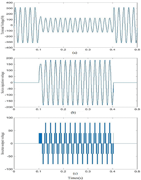
Fig. 4. During voltage sag (a) grid terminal voltage (vt), (b) series injected
voltage (vinj) and (c) inverter terminal voltage (vinv).


Fig. 5. FFT analysis of the series injected voltage (vinj).

Fig. 6. (a) Grid terminal voltage and (b) load voltage during Voltage flicker

CONCLUSION
This paper proposes dynamic voltage restorer based on the ground point shifting multilevel Inverter topology (GPSMI). The operation of the multilevel inverter and the power circuit diagram is explained. The inverter topology requires less number of switches than conventional multi-level inverter. In this inverter topology, only two switches are active at any instant of time that reduce switch conduction loss. The passive filter requirement in the DVR topology is reduced by using this multi-level inverter. Proper PWM for this proposed inverter has been explained. Instantaneous sag identification technique using d-q reference frame has also been explained. This proposed DVR can mitigate the power quality problem like sag/swell and voltage flicker.
REFERENCES

[1] IEEE Guide for Voltage Sag Indices,” in IEEE Std 1564-2014 , vol., no., pp.1-59, June 20 2014
[2] IEEE Guide for Identifying and Improving Voltage Quality in Power Systems,” in IEEE Std 1250-2011 (Revision of IEEE Std 1250-1995) , vol., no., pp.1-70, March 31 2011
[3] A. Ghosh and G. Ledwich, ”Structures and control of a dynamic voltage regulator (DVR),” Power Engineering Society Winter Meeting, 2001. IEEE, Columbus, OH, 2001, pp. 1027-1032 vol.3. doi: 10.1109/PESW.2001.917209
[4] Huiwen Liu, Bowen Zheng and Xiong Zhan, ”A comparison of two types of storageless DVR with a passive shunt converter,” 2016 IEEE 8th International Power Electronics and Motion Control Conference (IPEMC-ECCE Asia), Hefei, 2016, pp. 1280-1284.
[5] P. C. Loh, D. M. Vilathgamuwa, S. K. tang, H. L. Long, ”Multilevel dynamic voltage restorer”, IEEE Power Electronic Letters, vol. 2, no. 4, pp. 125-130, Dec. 2004.