asokatechnologies@gmail.com 09347143789/09949240245

Search This Blog

Tuesday 18 April 2017

An Improved Modulated Carrier Control with On-Time Doubler for Single-Phase Shunt Active Power Filter


ABSTRACT
This paper proposes an improved modulated carrier control with on-time doubler for the single-phase shunt active power filter, which eliminates harmonic and reactive currents drawn by nonlinear loads. This control method directly shapes the line current to be sinusoidal and in phase with the grid voltage by generating a modulated carrier signal with a resettable integrator, comparing the carrier signal to the average line current and making duty ratio doubled. Since the line current compared to the carrier signal is not the peak, but the average value, dc-offset appeared at the conventional control methods based on one-cycle control is effectively addressed. The proposed control technique extirpates the harmonic and reactive currents and solves the dc-offset problem. The operation principle and stability characteristic of the single-phase shunt active power filter with the proposed control method are discussed, and experimental results with laboratory prototype under various load conditions verify its performance.

KEYWORDS
1.      Single-phase shunt active power filter
2.      Modulated carrier control
3.      Indirect control
4.      One-cycle control
5.      Harmonic and reactive currents elimination
6.      Nonlinear load.

SOFTWARE: MATLAB/SIMULINK

CIRCUIT DIAGRAM
Fig. 1. Single-phase shunt active power filter with nonlinear load.
Fig. 2. Overall control structure of the proposed control method with the shunt APF.

EXPECTED SIMULATION RESULTS
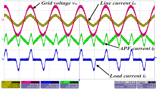
Fig. 3. Measured grid voltage, line current, APF current and load current waveforms of the shunt APF system based on the proposed control method at full load condition (vin : 200 V/div, iin : 20 A/div, if : 20 A/div, i- L : 20 A/div).

Fig. 4. Measured grid voltage, line current, APF current and load current waveforms of the shunt APF system based on the proposed control method at half load condition (vin : 200 V/div, iin : 20 A/div, if : 20 A/div, iL : 20 A/div).


Fig. 5. Current controller switching mechanism.
Fig. 6. Measured dc-link voltage, line current, APF current and load current waveforms of the shunt APF system in load transient from 800 W to 1600 W (vo : 100 V/div, iin : 20 A/div, if : 20 A/div, iL : 20 A/div).

Fig. 7. Measured grid voltage, line current, APF current and load current waveforms of the shunt APF system at 110 Vrms grid voltage. (vin : 100 V/div, iin : 10 A/div, if : 10 A/div, iL : 10 A/div) Under (a) 200 W, (b) 270 W, (c) 340 W, (d) 400 W load condition

Fig. 8. Power factors of the nonlinear load system with and without the APF under various load conditions.

CONCLUSION
An improved modulated carrier control for single-phase active power filter has been proposed. The shunt APF with the proposed control method fulfills harmonic and reactive current elimination at the line current by comparing the carrier signal to the average line current and having the duty ratio doubled. On top of that, the control method totally gets rid of the dc-offset problem arisen at the conventional one based on one-cycle control and ameliorates the current control loop stability without additional ramp signal. The operation principle of power stage, the main control mechanism, and the stability characteristic of the current control loop are analyzed in detail. Experimental results with the shunt APF system under assorted conditions verify the performance of the proposed control method in steady and transient states.

REFERENCES
[1]         Elham B. Makram, E.V. Subramaniam, Adly A. Girgis, and Ray Catoe, “Hamonic filter design using actual recorded data,” IEEE Transaction on Industrial Application, vol. 29, no. 6, pp. 1176-1183, Nov. 1993.
[2]         F. Z. Peng, “Harmonic sources and filtering approaches,” IEEE Transaction on Industrial Application Magazine, vol. 7, no. 4, pp. 18-25, Jul. /Aug. 2001.
[3]         Czarnecki, L. S., Ginn, H. L., “The effect of the design method on efficiency of resonant harmonic filters,” IEEE Transactions on Power Delivery, vol. 20, no. 1, pp. 286-291, Jan. 2005.
[4]         Fakhralden A. Huliehel, Fred C. Lee, and Bo H. Cho, “Small-signal modeling of the single-phase boost high power factor converter with constant frequency control,” PESC’92 Record. 23rd annual IEEE Power electronics Specialists Conference, 1992, vol.1, pp. 475 – 482.

[5]         R. Martinez, P. N. Enjeti, “A high-performance single-phase rectifier with input power factor correction,” IEEE Transactions on Power Electronics, vol. 11, no. 2, pp. 311–317, Mar. 1996.

An Integrated Dynamic Voltage Restorer Ultra-capacitor Design for Improving Power Quality of the Distribution Grid


ABSTRACT
Cost of various energy storage technologies is decreasing rapidly and the integration of these technologies into the power grid is becoming a reality with the advent of smart grid. Dynamic voltage restorer (DVR) is one product that can provide improved voltage sag and swell compensation with energy storage integration. Ultra-capacitors (UCAP) have low-energy density and high-power density ideal characteristics for compensation of voltage sags and voltage swells, which are both events that require high power for short spans of time. The novel contribution of this paper lies in the integration of rechargeable UCAP-based energy storage into the DVR topology. With this integration, the UCAP-DVR system will have active power capability and will be able to independently compensate temporary voltage sags and swells without relying on the grid to compensate for faults on the grid like in the past. UCAP is integrated into dc-link of the DVR through a bidirectional dc–dc converter, which helps in providing a stiff dc-link voltage, and the integrated UCAP-DVR system helps in compensating temporary voltage sags and voltage swells, which last from 3 s to 1 min. Complexities involved in the design and control of both the dc–ac inverter and the dc–dc converter are discussed. The simulation model of the overall system is developed.

 KEYWORDS
1.      Digital Signal Processing (DSP)
2.      Dynamic voltage restorer (DVR)
3.      Energy storage integration
4.      Phase locked loop (PLL)
5.      Ultracapacitor (UCAP).

SOFTWARE: MATLAB/SIMULINK

BLOCK DIAGRAM

Fig. 1. One-line diagram of DVR with UCAP energy storage.

Fig. 2. Model of three-phase series inverter (DVR) and its controller with
integrated higher order controller.

  
EXPECTED SIMULATION RESULTS
Fig. 4. (a) Source and load RMS voltages Vsrms and VLrms during sag.(b) Source voltages Vsab (blue), Vsbc (red), and Vsca (green) during sag. (c) Load voltages VLab (blue), VLbc (red), and VLca (green) during sag. (d) Injected voltages Vinj2a (blue), Vinj2b (red), and Vinj2c (green) during sag. (e) Vinj2a (green) and Vsab (blue) waveforms during sag.
Fig. 5. (a) Currents and voltages of dc–dc converter. (b) Active power of grid, load, and inverter during voltage sag.
Fig. 6. (a) Source and load rms voltages Vsrms and VLrms during swell. (b) Source voltages Vsab (blue), Vsbc (red), and Vsca (green) during swell. (c) Load voltages VLab (blue), VLbc (red), and VLca (green) during swell. (d) Injected voltages Vinj2a (blue), Vinj2b (red), Vinj2c (green) during swell. (e) Vinj2a (green) and Vsab (blue) waveforms during swell.
Fig. 7. (a) Currents and voltages of dc–dc converter during swell. (b) Active and reactive power of grid, load, and inverter during a voltage swell.
Fig. 8. (a) UCAP and bidirectional dc–dc converter simulation waveforms Ecap (CH1), Vfdc (CH2), Idclnk (CH3) and Iucav (CH4) during voltage sag. (b) Inverter simulation waveforms Vsab (CH1), VLab (CH2) and Vinj2a (CH3) and ILa (CH4) during the voltage sag.
Fig. 9. (a) UCAP and dc–dc converter simulation waveformsEcap (CH1), Vfdc (CH2), Idclnk (CH3), and Iucav (CH4) during voltage swell. (b) Inverter simulation waveforms Vsab (CH1), VLab (CH2) and Vinj2a (CH3) and ILa (CH4) during the voltage swell.
Fig. 10. (a) Inverter experimental waveforms VLab (CH1), Vsa (CH2), Vsb (CH3), and ILa (CH4) for during an unbalanced sag in phases a and b. (b) Bidirectional dc–dc converter waveforms Ecap (CH1), Vfdc (CH2), Idclnk (CH3), and Iucav (CH4) showing transient response during an unbalanced sag in phases a and b.

CONCLUSION
In this paper, the concept of integrating UCAP-based rechargeable energy storage to the DVR system to improve its voltage restoration capabilities is explored. With this integration, the DVR will be able to independently compensate voltage sags and swells without relying on the grid to compensate for faults on the grid. The UCAP integration through a bidirectional dc–dc converter at the dc-link of the DVR is proposed. The power stage and control strategy of the series inverter, which acts as the DVR, are discussed. The control strategy is simple and is based on injecting voltages in-phase with the system voltage and is easier to implement when the DVR system has the ability to provide active power. A higher level integrated controller, which takes decisions based on the system parameters, provides inputs to the inverter and dc–dc converter controllers to carry out their control actions. Designs of major components in the power stage of the bidirectional dc–dc converter are discussed. Average current mode control is used to regulate the output voltage of the dc–dc converter due to its inherently stable characteristic.
The simulation of the UCAP-DVR system, which consists of the UCAP, dc–dc converter, and the grid-tied inverter, is carried out using PSCAD. Hardware experimental setup of the integrated system is presented and the ability to provide temporary voltage sag and swell compensation in all three phases to the distribution grid dynamically is tested. Results for transient response during voltage sags/swells in two phaseswill be included in the full-version of this paper. Results from simulation and experiment agree well with each other thereby verifying the concepts introduced in this paper. Similar UCAPbased energy storages can be deployed in the future on the distribution grid to respond to dynamic changes in the voltage profiles of the grid and prevent sensitive loads from voltage disturbances.

REFERENCES
[1]         N. H. Woodley, L. Morgan, and A. Sundaram, “Experience with an inverter-based dynamic voltage restorer,” IEEE Trans. Power Del., vol. 14, no. 3, pp. 1181–1186, Jul. 1999.
[2]         S. S. Choi, B. H. Li, and D.M. Vilathgamuwa, “Dynamic voltage restoration with minimum energy injection,” IEEE Trans. Power Syst., vol. 15, no. 1, pp. 51–57, Feb. 2000.
[3]         D. M. Vilathgamuwa, A. A. D. R. Perera, and S. S. Choi, “Voltage sag compensation with energy optimized dynamic voltage restorer,” IEEE Trans. Power Del., vol. 18, no. 3, pp. 928–936, Jul. 2003.
[4]         Y. W. Li, D. M. Vilathgamuwa, F. Blaabjerg, and P. C. Loh “A robust control scheme for medium-voltage-level DVR implementation,” IEEE Trans. Ind. Electron., vol. 54, no. 4, pp. 2249–2261, Aug. 2007.

[5]         A. Ghosh and G. Ledwich, “Compensation of distribution system voltage using DVR,” IEEE Trans. Power Del., vol. 17, no. 4, pp. 1030–1036, Oct. 2002.

Wednesday 12 April 2017

An Efficient High-Step-Up Interleaved DC–DC Converter with a Common Active Clamp


ABSTRACT:
This paper presents a high-efficiency and high-step up non isolated interleaved dc–dc converter with a common active clamp circuit. In the presented converter, the coupled-inductor boost converters are interleaved. A boost converter is used to clamp the voltage stresses of all the switches in the interleaved converters, caused by the leakage inductances present in the practical coupled inductors, to a low voltage level. The leakage energies of the interleaved converters are collected in a clamp capacitor and recycled to the output by the clamp boost converter. The proposed converter achieves high efficiency because of the recycling of the leakage energies, reduction of the switch voltage stress, mitigation of the output diode’s reverse recovery problem, and interleaving of the converters. Detailed analysis and design of the proposed converter are carried out. A prototype of the proposed converter is developed, and its experimental results are presented for validation.

KEYWORDS
1.      Active-clamp
2.      Boost converter
3.      Coupled-inductor boost converter
4.       Dc–dc power converter
5.       High voltage gain
6.      Interleaving

SOFTWARE: MATLAB/SIMULINK

CIRCUIT DIAGRAM:


Fig. 1. (a) Parallel diode clamped coupled-inductor boost converter and (b) proposed interleaved coupled-inductor boost converter with single boost converter clamp (for n = 3).


EXPECTED SIMULATION RESULTS:


Fig. 2. (a) Drain-to-source voltage of the switch in a coupled-inductor boost converter without any clamping and (b) output voltage, clamp voltage and drain to- source voltage of the switch in a coupled-inductor boost converter with the proposed active-clamp circuit.

.


Fig. 3. (a) From top to bottom: total input current of the converter, input currents of the interleaved coupled-inductor boost converters, and (b) primary current, secondary current, and leakage current in a phase of the interleaved coupled-inductor boost converters.


Fig. 4. (a) Gate pulses to the clamp boost converter and (b) inductor current of the clamp boost converter.


Fig. 5. Gate pulses to the interleaved coupled-inductor boost converters (10 V/div).

CONCLUSION:

Coupled-inductor boost converters can be interleaved to achieve high-step-up power conversion without extreme duty ratio operation while efficiently handling the high-input current. In a practical coupled-inductor boost converter, the switch is subjected to high voltage stress due to the leakage inductance present in the non ideal coupled inductor. The presented active clamp circuit, based on single boost converter, can successfully reduce the voltage stress of the switches close to the low-level voltage stress offered by an ideal coupled-inductor boost converter. The common clamp capacitor of this active-clamp circuit collects the leakage energies from all the coupled-inductor boost converters, and the boost converter recycles the leakage energies to the output. Detailed analysis of the operation and the performance of the proposed converter were presented in this paper. It has been found that with the switches of lower voltage rating, the recovered leakage energy, and the other benefits of an ideal coupled-inductor boost converter and interleaving, the converter can achieve high efficiency for high-step-up power conversion. A prototype of the converter was built and tested for validation of the operation and performance of the proposed converter. The experimental results agree with the analysis of the converter operation and the calculated efficiency of the converter.

 REFERENCES:

[1] L. Solero, A. Lidozzi, and J. A. Pomilio, “Design of multiple-input power converter for hybrid vehicles,” IEEE Trans. Power Electron., vol. 20, no. 5, pp. 107–116, Sep. 2005.
[2] A. A. Ferreira, J. A. Pomilio, G. Spiazzi, and de Araujo Silva, “Energy management fuzzy logic supervisory for electric vehicle power supplies system,” IEEE Trans. Power Electron., vol. 20, no. 1, pp. 107–115, Jan. 2008.
[3] A. Emadi, K. Rajashekara, S. S. Williamson, and S. M. Lukic, “Topological overview of hybrid electric and fuel cell vehicular power system architectures and configurations,” IEEE Trans. Veh. Technol., vol. 54, no. 3, pp. 763–770, May 2007.
[4] J. Bauman and M. Kazerani, “A comparative study of fuel cell-battery, fuel cell-ultracapacitor, and fuel cell-battery-ultracapacitor vehicles,” IEEE Trans. Veh. Technol., vol. 57, no. 2, pp. 760–769, Mar. 2008.

[5] Q. Zhao and F. C. Lee, “High-efficiency, high step-up DC–DC converters,” IEEE Trans. Power Electron., vol. 18, no. 1, pp. 65–73, Jan. 2003.

Tuesday 11 April 2017

Speed Controller of Switched Reluctance Motor


ABSTRACT
Fuzzy logic control has become an important methodology in control engineering. The paper proposes a Fuzzy Logic Controller (FLC) for controlling a speed of SRM drive. The objective of this work is to compare the operation of P& PI based conventional controller and Artificial Intelligence (AI) based fuzzy logic controller to highlight the performances of the effective controller. The present work concentrates on the design of a fuzzy logic controller for SRM speed control. The result of applying fuzzy logic controller to a SRM drive gives the best performance and high robustness than a conventional P & PI controller. Simulation is carried out using Matlab/Simulink.

KEYWORDS: P Controller, PI Controller, Fuzzy Logic Controller, Switched Reluctance Motor

SOFTWARE: MATLAB/SIMULINK

BLOCK DIAGRAM

Figure 1. Block diagram of SRM speed control


SIMULATION MODELS
Figure 2. Simulation model using P controller
Figure 3. Simulation model using PI controller.
Figure 4. Simulink model using FLC.

SIMULATION RESULTS
Figure 5. Output flux.


Figure 6. Output current

Figure 7. Output torque.
Figure 8. Speed.

CONCLUSION
Thus the SRM dynamic performance is forecasted and by using MATLAB/simulink the model is simulated. SRM has been designed and implemented for its speed control by using P, PI controller and AI based fuzzy logic controller. We can conclude from the simulation results that when compared with P & PI controller, the fuzzy Logic Controller meet the required output. This paper presents a fuzzy logic controller to ensure excellent reference tracking of switched reluctance motor drives. The fuzzy logic controller gives a perfect speed tracking without overshoot and enchances the speed regulation. The SRM response when controlled by FLC is more advantaged than the conventional P& PI controller.

REFERENCES
[1]         Susitra D, Jebaseeli EAE, Paramasivam S. Switched reluctance generator - modeling, design, simulation, analysis and control -a comprehensive review. Int J Comput Appl. 2010; 1(210):975–8887.
[2]         Susitra D., Paramasivam S. Non-linear flux linkage modeling of switched reluctance machine using MVNLR and ANFIS. Journal of Intelligent and Fuzzy Systems. 2014; 26(2):759–768.
[3]         Susitra D, Paramasivam S. Rotor position estimation for a switched reluctance machine from phase flux linkage. IOSR–JEEE. 2012 Nov–Dec; 3(2):7.
[4]         Susitra D, Paramasivam S. Non-linear inductance modeling of switched reluctance machine using multivariate non- linear regression technique and adaptive neuro fuzzy inference system. CiiT International Journal of Artificial Intelligent Systems and Machine Learning. 2011 Jun; 3(6).
[5]         Ramya A, Dhivya G, Bharathi PD, Dhyaneshwaran R, Ramakrishnan P. Comparative study of speed control of 8/6 switched reluctance motor using pi and fuzzy logic controller. IJRTE; 2012