ABSTRACT:
Two variants of the full soft-switching high step-up
DC-DC converter are proposed. The main advantage of the converters is the
minimized conduction losses by the use of the four-quadrant switches and a
specific control algorithm. Simulation was performed to verify the principle of
operation and to estimate the losses.
KEYWORDS:
1.
DC-DC power converters
2.
Photovoltaic systems
3.
Soft switching
4.
Step-up
5.
Isolated
SOFTWARE: MATLAB/SIMULINK
CIRCUIT DIAGRAM:

Fig.
1. Full soft-switching high step-up DC-DC converter

Fig.
2. Proposed converter topology with four four-quadrant switches.
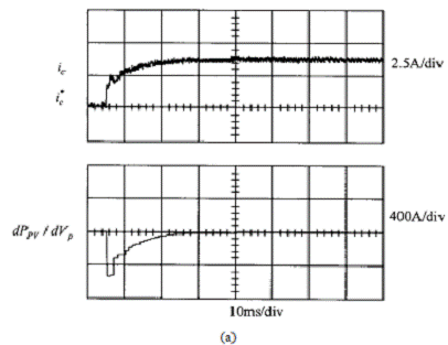
EXPECTED SIMULATION RESULTS:

Fig. 3. Simulated voltage and current
waveforms of S1 (a), S2 (b), S7.1 (c), S5 (d) for the proposed converter
topology with a single four-quadrant switch
CONCLUSION:
The
proposed converters allow soft-switching of the both inverter and rectifier
switches without any auxiliary passive elements and clamping circuits.
As
seen from simulation results, the topology with a single four-quadrant switch
has higher efficiency than the topology with four four-quadrant switches, but
at the same time, it has few disadvantages that could affect the final choice
of topology:
-
Step-up factor is slightly lower than in the topology with four four-quadrant
switches;
-
The switching interval e (and the symmetrical interval in another half-period)
must be of strictly right duration, which is equal to the time of current
redistribution between switches S4 and S2. The shorter duration of this
interval will result in high switching losses and, in extreme cases, can lead
to damage of the switch S4. The significantly longer duration will result in
current increase through the switch S2 and eventually may result in the boost
inductor saturation.
-
The original topology and the topology with four four quadrant switches does
not have the problem with the longer duration of this switching interval and so
they have lower requirements to the control system in dynamic mode. This means
that proposed converter with four four-quadrant switches allows robust
soft-switching commutation, which is hard to achieve in galvanically isolated
current-fed DCDC converters.
The main disadvantage of the topologies is the
presence of four switches in series in the inverter stage on the path of the current
flow during the energy transfer interval. This leads to the conduction losses
higher than in the conventional phase shifted full-bridge topology.
Nevertheless the switching losses are lower due to the introduced
soft-switching. It means that switching frequency could be increased while
maintaining the efficiency at acceptable level.
Future work will be devoted to the experimental verification
of the proposed converters and further control algorithm optimization.
REFERENCES:
[1]
A. Blinov, D. Vinnikov, and V. Ivakhno, “Full soft-switching high stepup dc-dc
converter for photovoltaic applications,” 2014 16th European Conference on
Power Electronics and Applications (EPE’14-ECCE Europe), pp. 1–7, Aug 2014.
[2]
Y. Sokol, Y. Goncharov, V. Ivakhno, V. Zamaruiev, B. Styslo, M. Mezheritskij,
A. Blinov, and D. Vinnikov, “Using the separated commutation in two-stage dc/dc
converter in order to reduce of the power semiconductor switches’ dynamic
losses,” Energy Saving. Power Engineering. Energy Audit, 2014.
[3]
A. Blinov, V. Ivakhno, V. Zamaruev, D. Vinnikov, and O. Husev, “Experimental
verification of dc/dc converter with full-bridge active rectifier,” 38th Annual
Conference on IEEE Industrial Electronics Society (IECON 2012), pp. 5179–5184 ,
Oct 2012.
[4]
R.-Y. Chen, T.-J. Liang, J.-F. Chen, R.-L. Lin, and K.-C. Tseng, “Study and
implementation of a current-fed full-bridge boost dc-dc converter with
zero-current switching for high-voltage applications,” IEEE Transactions on
Industry Applications, vol. 44, no. 4, pp. 1218–1226, July 2008.
[5]
J.-F. Chen, R.-Y. Chen, and T.-J. Liang, “Study and implementation of a single-stage
current-fed boost pfc converter with zcs for high voltage applications,” IEEE
Transactions on Power Electronics, vol. 23, no. 1, pp. 379–386, Jan 2008.