Enhancing
power cycling capability of power semiconductor devices is highly demanded in order
to increase the long term reliability of multilevel inverters. Ageing of power
switches and their cooling systems leads to their accelerated damage due to
excess power losses and junction temperatures. Therefore, thermal stresses
relief (TSR) is the most effective solution for lifetime extension of power
semiconductor devices. This paper presents a new thermal stresses relief
carrier-based pulse width modulation (TSRPWM) strategy for extending the
lifetime of semiconductor switches in single-phase multilevel inverters. The
proposed strategy benefits the inherent redundancy among switching states in
multilevel inverters to optimally relieve the thermally stressed device. The
proposed algorithm maintains the inverter operation without increased stresses on
healthy switches and without reduction of the output power ratings. In
addition, the proposed algorithm preserves voltage balance of the DC-link
capacitors. The proposed strategy is validated on single phase five level
T-type inverter system with considering different locations of thermal stresses
detection. Experimental prototype of the selected case study is built to verify
the results. Moreover, comparisons with the most featured strategies in
literature are given in detail.
KEYWORDS:
1. Lifetime extension
2. long term
reliability
3. multilevel inverter
4. pulse width
modulation (PWM)
5. thermal stresses relief
SOFTWARE: MATLAB/SIMULINK
BLOCK DIAGRAM

Fig.
1. A schematic diagram of PWM controlled full bridge n-level T-type
inverter
.
EXPECTED SIMULATION RESULTS

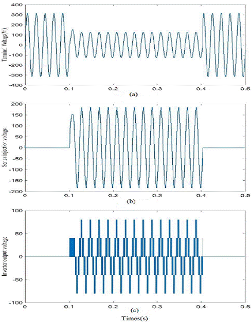
Fig.
2. Simulation results of the proposed strategy at TSD in SA11 at mi=0.85.


Fig.
4. Simulation results of the proposed TSRPWM strategy at TSD in SA12 and
mi=0.85.
CONCLUSION
This
paper has proposed a new carrier-based modulation strategy, called TSRPWM, for
single phase multilevel inverters. It retains the same benefits as the conventional
carrier PWM methods, i.e., a simple and easy implementation, but presents a
significantly reduced power losses and thermal stresses of the stressed
semiconductor devices. The main idea of the new proposed strategy is adaptively
selecting the redundant switching states in each switching cycle, in order to
optimize power losses through the thermally-stressed device. Therefore, both of
the junction temperature and temperature cycling of the stressed device are
reduced by the proposed strategy compared with normal mode operation of the
device. The results of simulation and experimental prototypes are conformed and
verified the new proposed concept. A generalized implementation of the proposed
TSRPWM, to provide thermal stresses relief for any of the components and for
any n-level inverters, is also presented. Moreover, the proposed strategy
maintains the inverter operation with the same output ratings, and voltage
balance over DC-link capacitors. Finally, the performance of the proposed
strategy is compared with the prominent strategies in literature, and the
distinction of the proposed strategy has become clear.
REFERENCES
[1] Shaoyong Yang,
A. Bryant, P. Mawby, Dawei Xiang, Li Ran, and P. Tavner, “An industry-based
survey of reliability in power electronic converters,” IEEE Trans. Ind.
Appl., vol. 47, no. 3, pp. 1441–1451, May 2011.
[2] S. E. De
Leon-Aldaco, H. Calleja, and J. Aguayo Alquicira, “Reliability and mission
profiles of photovoltaic systems: a FIDES approach,” IEEE Trans. Power
Electron., vol. 30, no. 5, pp. 2578–2586, May 2015.
[3] B. Ji, X.
Song, E. Sciberras, W. Cao, Y. Hu,0 and V. Pickert, “Multiobjective design
optimization of IGBT power modules considering power cycling and thermal
cycling,” IEEE Trans. Power Electron., vol. 30, no. 5, pp. 2493–2504,
May 2015.
[4] U.-M. Choi, F.
Blaabjerg, and K.-B. Lee, “Study and handling methods of power IGBT module failures
in power electronic converter systems,” IEEE Trans. Power Electron.,
vol. 30, no. 5, pp. 2517–2533, May 2015.
[5]
P. A. Mawby, W. Lai, H. Qin, O. Alatise, S. Xu, M. Chen, and L. Ran, “Study on
the lifetime characteristics of power modules under power cycling conditions,” IET
Power Electron., vol. 9, no. 5, pp. 1045–1052, Apr. 2016.