asokatechnologies@gmail.com 09347143789/09949240245

Search This Blog

Wednesday, 29 June 2016

New AC-DC Power Factor Correction Architecture Suitable for High Frequency Operation


ABSTRACT:

This paper presents a novel ac-dc power factor correction (PFC) power conversion architecture for single-phase grid interface. The proposed architecture has significant advantages for achieving high efficiency, good power factor, and converter miniaturization, especially in low-to-medium power applications. The architecture enables twice-line-frequency energy to be buffered at high voltage with a large voltage swing, enabling reduction in the energy buffer capacitor size, and elimination of electrolytic capacitors. While this architecture can be beneficial with a variety of converter topologies, it is especially suited for system miniaturization by enabling designs that operate at high frequency (HF, 3 – 30 MHz). Moreover, we introduce circuit implementations that provide efficient operation in this range. The proposed approach is demonstrated for an LED driver converter operating at a (variable) HF switching frequency (3 – 10 MHz) from 120Vac, and supplying a 35Vdc output at up to 30W. The prototype converter achieves high efficiency (92 %) and power factor (0.89), and maintains good performance over a wide load range. Owing to architecture and HF operation, the prototype achieves a high ‘box’ power density of 50W/ in3 (‘displacement’ power density of 130W/ in3), with miniaturized inductors, ceramic energy buffer capacitors, and a small-volume EMI filter.

KEYWORDS:
1.      AC-DC
2.       High frequency
3.       Buck
4.       Power factor correction
5.      PFC
6.       Power factor
7.       LED
8.       Electromagnetic interference
9.      EMI

SOFTWARE: MATLAB/SIMULINK

BLOCK DIAGRAM:


Fig. 1: The proposed grid interface power conversion architecture comprises a line-frequency rectifier, a stack of capacitors, a set of regulating converters, and a power combining converter.

EXPECTED SIMULATION RESULTS:


Fig. 2: Operation of the prototype converter from a 120Vac line voltage to a 35Vdc output. Each figure illustrates voltage and / or current waveforms over the ac line cycle: (a) the measured 120Vac line input voltage and the measured voltages across the capacitor stack (output of the bridge rectifier) (b) the measured voltages across C1 and across C2 for a delivered output power of 29W (c) the measured input current waveform
at 29W output power (d) the measured input current waveform at 20W output power (e) the output voltage waveform at 29W output power (f) the switched capacitor voltage waveform at 29W output power.
             

CONCLUSION:

A new single-phase grid interface ac-dc PFC architecture is introduced and experimentally demonstrated. In addition to enabling high efficiency and good power factor, this PFC architecture is particularly advantageous in that it enables extremely high operating frequencies (into the HF range) and reduction in energy buffer capacitor values, each of which contributes to converter miniaturization. The proposed stacked combined architecture significantly decreases the voltage stress of the active and passive devices and reduces characteristic impedance levels, enabling substantial increases in switching frequency when utilized with appropriate converter topologies. Moreover, good power factor is achieved while dynamically buffering twice-line-frequency ac energy with relatively small capacitors operating with large voltage swing. The prototype converter achieves high efficiency and good power factor over a wide power range, and meets the CISPR Class-B Conducted electromagnetic interference (EMI) Limits. The


Fig. 3: The proposed architecture can be extended to more than two capacitors in the capacitor stack and other correspondingly other system blocks. This is particularly useful for handling universal ac line interface. Moreover, the number of capacitors and sub-regulating converter may be allowed to vary dynamically depending upon whether the circuit is connected to 120 or 240 Vac.


Fig. 4: The stack of flyback converters can regulate output load voltage and combine power to supply single load with connected secondary wires. Two flyback converters need to be modulated over the line cycle to achieve high power factor and buffer ac energy.
prototype converter based on the architecture and selected high-frequency circuit topology demonstrates an approximate factor of 10 reduction in volume compared to typical designs. The prototype has a very high ‘box’ power density of 50W=in3 (‘displacement’ power density of 130W=in3) with miniaturized inductors, a small volume of EMI filter, and ceramic energy buffer capacitors. Lastly, as described in the appendix, the proposed architecture can be realized in various ways (e.g., with alternative topologies) to realize features such as galvanic isolation and universal input range.

REFERENCES:
[1] O. Garcia, J. Cobos, R. Prieto, P. Alou, and J. Uceda, “Single phase power factor correction: a survey,” Power Electronics, IEEE Transactions on, vol. 18, no. 3, pp. 749–755, May 2003.
[2] G. Moschopoulos and P. Jain, “Single-phase single-stage power-factor corrected converter topologies,” Industrial Electronics, IEEE Transactions on, vol. 52, no. 1, pp. 23–35, Feb 2005.
[3] B. Singh, B. Singh, A. Chandra, K. Al-Haddad, A. Pandey, and D. Kothari, “A review of single-phase improved power quality ac-dc converters,” Industrial Electronics, IEEE Transactions on, vol. 50, no. 5, pp. 962–981, Oct 2003.
[4] Energy Star, “Energy star program requirements for integral LED lamps,” Energy Star, Tech. Rep., Aug. 2010.
[5] ——, “Energy star program requirements for computers,” Energy Star, Tech. Rep., Jun. 2014.
[6] D. Perreault, J. Hu, J. Rivas, Y. Han, O. Leitermann, R. Pilawa- Podgurski, A. Sagneri, and C. Sullivan, “Opportunities and challenges in very high frequency power conversion,” in Applied Power Electronics Conference and Exposition, 2009. APEC 2009. Twenty-Fourth Annual IEEE, Feb 2009, pp. 1–14.


A High Step-Up Converter with Voltage-Multiplier Modules for Sustainable Energy Applications


ABSTRACT
This paper proposes a novel isolated high step-up converter for sustainable energy applications. Through an adjustable voltage-multiplier module, the proposed converter achieves a high step-up gain without utilizing either a large duty ratio or a high turns ratio. The voltage-multiplier modules are composed of coupled inductors and switched capacitors. Due to the passive lossless clamped performance, leakage energy is recycled, which alleviates a large voltage spike across the main switches and improves efficiency. Thus, power switches with low levels of voltage stress can be adopted for reducing conduction losses. In addition, the isolated topology of the proposed converter satisfies electrical-isolation and safety regulations. The proposed converter also possesses continuous and smooth input current, which decreases the conduction losses, lengthens life time of the input source, and constrains conducted electromagnetic-interference problems. Finally, a prototype circuit with 40 V input voltage, 380 V output, and 500 W maximum output power is operated to verify its performance. The maximum efficiency is 94.71 % at 200 W, and the full-load efficiency is 90.67 % at 500 W.

KEYWORDS
1.      High Step-Up
2.      Voltage-Multiplier Module
3.      Isolated Converter

SOFTWARE: MATLAB/SIMULINK

BLOCK DIAGRAM:

Fig. 1. Block diagram of a typically sustainable energy system.

Fig. 2. Proposed isolated high step-up converter for sustainable energy applications.

 EXPERIMENTAL RESULTS:

(a) Measured waveforms of vDS1, vDS2, iLin and iLk

(b) Measured waveforms of vDc, vDr and iDr

(C)Measured waveforms of vDf1, vDf2, iDf1 and iDf2

(d) Measured waveforms of vDo, iDo and Vo
Fig.3 The experimental waveforms measured at a full load of 500 W.

CONCLUSION
This paper has presented the theoretical analysis of steady-state and experimental results for the proposed converter, which successfully demonstrates its performance. A prototype isolated converter has been successfully implemented with a high step-up ratio and high efficiency for sustainable energy applications. The presented circuit topology inherently makes the input current continuous and smooth, which decreases the conduction losses, lengthens the life time of the input source, and constrains conducted EMI problems. In addition, the lossless passive clamp function recycles the leakage energy and constrains/lowers the voltage spikes across the power switches. Meanwhile, the voltage stress on the power switch is restricted and is much lower than the output voltage Vo, which is 380 V. Furthermore, the full-load efficiency is 90.67% at Po =500 W, and the maximum efficiency is 94.71% at Po = 200 W. Thus, the proposed converter is suitable for renewable-energy applications that need high step-up conversion and have electrical-isolation requirements.

REFERENCES

1.      T. Kefalas, and A. Kladas, “Analysis of transformers working under heavily saturated conditions in grid-connected renewable energy systems,” IEEE Trans. Ind. Electron., vol. 59, no. 5, pp. 2342–2350, May 2012.
2.      Jonghoon Kim, Jaemoon Lee, and B. H. Cho, “Equivalent circuit modeling of pem fuel cell degradation combined with a lfRC,” IEEE Trans. Ind. Electron., vol. 60, no. 11, pp. 5086–5094, Nov. 2013.
3.      Prasanna U R, and Akshay K. Rathore, “Extended range zvs active-clamped current-fed full-bridge isolated dc/dc converter for fuel cell applications: analysis, design, and experimental results,” IEEE Trans. Ind. Electron., vol. 60, no. 7, pp. 2661–2672, July 2013.
4.      Shih-Jen Cheng, Yu-Kang Lo, Huang-Jen Chiu, and Shu-Wei Kuo, “High-efficiency digital-controlled interleaved power converter for high-power pem fuel-cell applications,” IEEE Trans. Ind. Electron., vol. 60, no. 2, pp. 773–780, Feb. 2013.
5.      Changzheng Zhang, Shaowu Du, and Qiaofu Chen, “A novel scheme suitable for high-voltage and large-capacity photovoltaic power stations,” IEEE Trans. Ind. Electron., vol. 60, no. 9, pp. 3775–3783, Sept. 2013.


A High Gain Input-Parallel Output-Series DC/DC Converter with Dual Coupled Inductors

ABSTRACT
High voltage gain dc–dc converters are required in many industrial applications such as photovoltaic and fuel cell energy systems, high-intensity discharge lamp (HID), dc back-up energy systems, and electric vehicles. This paper presents a novel input-parallel output-series boost converter with dual coupled inductors and a voltage multiplier module. On the one hand, the primary windings of two coupled inductors are connected in parallel to share the input current and reduce the current ripple at the input. On the other hand, the proposed converter inherits the merits of interleaved series-connected output capacitors for high voltage gain, low output voltage ripple, and low switch voltage stress. Moreover, the secondary sides of two coupled inductors are connected in series to a regenerative capacitor by a diode for extending the voltage gain and balancing the primary-parallel currents. In addition, the active switches are turned on at zero current and the reverse recovery problem of diodes is alleviated by reasonable leakage inductances of the coupled inductors. Besides, the energy of leakage inductances can be recycled. A prototype circuit rated 500-W output power is implemented in the laboratory, and the experimental results shows satisfactory agreement with the theoretical analysis.

KEYWORDS
1.      DC–DC converter
2.      Dual coupled inductors
3.      High gain
4.      Input-parallel output-series.

SOFTWARE: MATLAB/SIMULINK
CIRCUIT DIAGRAM:

Fig. 1. Equivalent circuit of the presented converter.


Fig.2 Key theoretical waveforms.


EXPERIMENTAL VERIFICATIONS:


Fig.3 Key experimental current waveforms.

Fig.4 Voltage stress waveforms of power components.

CONCLUSION
For low input-voltage and high step up power conversion, this paper has successfully developed a high-voltage gain dc–dc converter by input-parallel output-series and inductor techniques. The key theoretical waveforms, steady-state operational principle, and the main circuit performance are discussed to explore the advantages of the proposed converter. Some important characteristics of the proposed converter are as follows: 1) it can achieve a much higher voltage gain and avoid operating at extreme duty cycle and numerous turn ratios; 2) the voltage stresses of the main switches are very low, which are one fourth of the output voltage under N = 1; 3) the input current can be automatically shared by each phase and low ripple currents are obtained at input; 4) the main switches can be turned ON at ZCS so that the main switching losses are reduced; and 5) the current falling rates of the diodes are controlled by the leakage inductance so that the diode reverse-recovery problem is alleviated. At the same time, there is a main disadvantage that the duty cycle of each switch shall be not less than 50% under the interleaved control with 180phase shift.

REFERENCES
[1] C.Cecati, F. Ciancetta, and P. Siano, “A multilevel inverter for photovoltaic systems with fuzzy logic control,” IEEE Trans. Ind. Electron., vol. 57, no. 12, pp. 4115–4125, Dec. 2010.
[2] X. H. Yu, C. Cecati, T. Dillon, and M. G. Simoes, “The new frontier of smart grid,” IEEE Trans. Ind. Electron. Mag., vol. 15, no. 3, pp. 49–63, Sep. 2011.
[3] G. Fontes, C. Turpin, S. Astier, and T. A. Meynard, “Interactions between fuel cell and power converters: Influence of current harmonics on a fuel cell stack,” IEEE Trans. Power Electron., vol. 22, no. 2, pp. 670–678, Mar. 2007.
[4] J. Y. Lee and S. N. Hwang, “Non-isolated high-gain boost converter using voltage-stacking cell,” Electron. Lett., vol. 44, no. 10, pp. 644–645, May 2008.

[5] Z. Amjadi and S. S. Williamson, “Power-electronics-based solutions for plug-in hybrid electric vehicle energy storage and management systems,” IEEE Trans. Ind. Electron., vol. 57, no. 2, pp. 608–616, Feb. 2010.

Tuesday, 28 June 2016

PV-Active Power Filter Combination Supplies Power to Nonlinear Load and Compensates Utility Current


ABSTRACT

The photovoltaic (PV) generation is increasingly popular nowadays, while typical loads require more high-power quality. Basically, one PV generator supplying to nonlinear loads is desired to be integrated with a function as an active power filter (APF). In this paper, a three-phase three-wire system, including a detailed PV generator, dc/dc boost converter to extract maximum radiation power using maximum power point tracking, and dc/ac voltage source converter to act as an APF, is presented. The instantaneous power theory is applied to design the PV-APF controller, which shows reliable performances. The MATLAB/Simpower Systems tool has proved that the combined system can simultaneously inject maximum power from a PV unit and compensate the harmonic current drawn by nonlinear loads.

KEYWORDS
1.      Active power filter (APF)
2.      Instantaneous power theory
3.      Photovoltaic (PV)
4.      Power quality
5.      Renewable energy

SOFTWARE: MATLAB/SIMLINK

 BLOCK DIAGRAM:

Figure 1. proposed design of PV-APF combination.

CONTROL DIAGRAM:

Figure 2. controller topology of dc/ac VSC in the PV-APF combination.

EXPECTED SIMULATION RESULTS:

Figure 3. output power of pv during running time.

Figure 4. duty cycle and vpv changed by mppt. (a) output
voltage of pv unit. (b) duty cycle of mppt.

Figure 5. utility supplied current waveform.

Figure 6. utility supplied current and pcc voltage waveform.

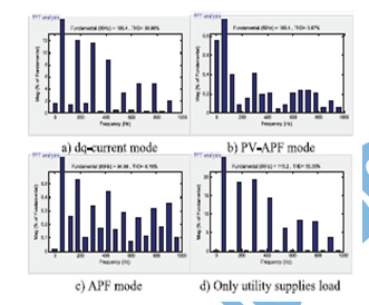
Figure 7. thd in four modes of pv system operation while
utility supplies power. (a) dq-current mode. (b) pv-apf mode.
(c) apf mode. (d) only utility supplies load.

Figure 8. pv supplied current waveform.

Figure 9. real power from the (a) utility, (b) pv unit, and (c)
load, while the utility supplies power.

Figure 10. imaginary power from the (a) utility, (b) pv unit,
and (c) load, while the utility supplies power.

Figure 11. utility received current waveform.


Figure 12. thd in four modes of pv system operation while
utility receives power. (a) dq-current mode. (b) pv-apf mode.
(c) apf mode. (d) only utility supplies load.


Figure 13. real power from the (a) utility, (b) pv unit, and (c)
load, while the utility receives power.

Figure 14. imaginary power from the (a) utility, (b) pv unit,
and (c) load, while the utility receives power.

CONCLUSION:

Regarding the multifunctional DG concept, in this paper, a dynamic grid-connected PV unit is built and the PV-APF combination system with a local controller is proposed. The controller implements two purposes, which are supplying power from the PV unit and filtering the harmonics of the local nonlinear load. The new controller based on instantaneous power balance has been explained accordingly. The MATLAB/Simpower Systems simulation shows good performances of this controller. The positive influence of MPPT on maximizing PV power output is also validated. The switching among three controllers to dc/ac VSC brings different current waveforms. As a result, the conventional dq-current controller should not be applied when PV is connected to a local nonlinear load regarding power-quality viewpoint. Preferably, the PV-APF controller compensates the utility currents successfully. While a PV unit is deactivated, the APF function can still operate. It is, therefore, technically feasible for these power electronics-interfaced DG units to actively regulate the power quality of the distribution system as an ancillary service, which will certainly make those DG units more competitive.

REFERENCES:

[1] L. Hassaine, E. Olias, J. Quintero, and M. Haddadi, ``Digital power factor control and reactive power regulation for grid-connected photovoltaic inverter,'' Renewable Energy, vol. 34, no. 1, pp. 315_321, 2009.
[2] N. Hamrouni, M. Jraidi, and A. Cherif, ``New control strategy for 2-stage grid-connected photovoltaic power system,'' Renewable Energy, vol. 33, no. 10, pp. 2212_2221, 2008.
[3] M. G. Villalva, J. R. Gazoli, and E. R. Filho, ``Comprehensive approach to modeling and simulation of photovoltaic arrays,'' IEEE Trans. Power Electron., vol. 24, no. 5, pp. 1198_1208, May 2009.
[4] N. R. Watson, T. L. Scott, and S. Hirsch, ``Implications for distribution networks of high penetration of compact _uorescent lamps,'' IEEE Trans. Power Del., vol. 24, no. 3, pp. 1521_1528, Jul. 2009.

[5] I. Houssamo, F. Locment, and M. Sechilariu, ``Experimental analysis of impact of MPPT methods on energy ef_ciency for photovoltaic power systems,'' Int. J. Elect. Power Energy Syst., vol. 46, pp. 98_107, Mar. 2013.