asokatechnologies@gmail.com 09347143789/09949240245

Search This Blog

Thursday, 6 April 2017

Full-Soft-Switching High Step-Up Bidirectional Isolated Current-Fed Push-Pull DC-DC Converter for Battery Energy Storage Applications


ABSTRACT
This paper presents a novel bidirectional current-fed push-pull DC-DC converter topology with galvanic isolation. The control algorithm proposed enables full-soft-switching of all transistors in a wide range of input voltage and power with no requirement for snubbers or resonant switching. The converter features an active voltage doubler rectifier controlled by the switching sequence synchronous to that of the input-side switches. As a result, full-soft-switching operation at a fixed switching frequency is achieved. Operation principle for the energy transfer in both directions is described, followed by verification with a 300 W experimental prototype. The converter has considerably higher voltage step-up performance than traditional current-fed converters Experimental results obtained are in good agreement with the theoretical steady-state analysis.

KEYWORDS
1.      Current-fed dc-dc converter
2.      Bidirectional converter
3.      Soft-switching
4.      ZVS
5.      ZCS
6.      Push-pull converter
7.      Switching control method

SOFTWARE: MATLAB/SIMULINK


CIRCUIT DIAGRAM
Fig. 1. Full-soft-switching CF push-pull converter proposed.

SIMULATION RESULTS
Fig. 2. Simulation current and voltage waveforms of the switch S1.1.

Fig. 3. Simulation current and voltage waveforms of the switch S1.2.

Fig. 4. Simulation current and voltage waveforms of the switch S4.

CONCLUSION
A novel bidirectional current-fed push-pull converter with galvanic isolation was introduced. It features full-softswitching operation of all semiconductor components, while its DC voltage gain is higher than in traditional current-fed converters due to the utilization of the circulating energy for the input voltage step-up. As a result, it does not suffer from short intervals of energy transfer from the input side to the output side since at least half of the switching period is dedicated for this. Moreover, it does not require any clamping circuits, since the novel control algorithm features natural clamping of the switches at the current-fed side. Despite a relatively high number of semiconductor components, it shows the peak efficiency of 96.3%, which does not depend on the energy transfer direction for the corresponding operating point. Soft-switching operation with continuous current at the currentfed side makes the converter proposed suitable for residential battery energy storage systems. Further research will be directed towards experimental verification of the converter performance with a lithium iron phosphate battery.

REFERENCES
[1]         F. Blaabjerg, and D.M. Ionel, "Renewable Energy Devices and Systems – State-of-the-Art Technology, Research and Development, Challenges and Future Trends," Electric Power Components and Systems, vol.43, no.12, pp.1319-1328, 2015.
[2]         C, Heymans, S, B. Walker, S. B. Young, M. Fowler, "Economic analysis of second use electric vehicle batteries for residential energy storage and load-levelling," Energy Policy, vol. 71, pp. 22-30, Aug. 2014.
[3]         J. Weniger, T. Tjaden, V. Quaschning, "Sizing of Residential PV Battery Systems," Energy Procedia, vol. 46, pp. 78-87,2014.
[4]         S. J. Chiang, K. T. Chang and C. Y. Yen, "Residential photovoltaic energy storage system," IEEE Trans. Ind. Electron., vol. 45, no. 3, pp. 385-394, Jun 1998.

[5]         S. X. Chen, H. B. Gooi and M. Q. Wang, "Sizing of Energy Storage for Microgrids," IEEE Trans. Smart Grid, vol. 3, no. 1, pp. 142-151, 2012.

Hybrid-Type Full-Bridge DC/DC Converter With High Efficiency


ABSTRACT:
This paper presents a hybrid-type full-bridge dc/dc converter with high efficiency. Using a hybrid control scheme with a simple circuit structure, the proposed dc/dc converter has a hybrid operation mode. Under a normal input range, the proposed converter operates as a phase-shift full-bridge series-resonant converter that provides high efficiency by applying soft switching on all switches and rectifier diodes and reducing conduction losses. When the input is lower than the normal input range, the converter operates as an active-clamp step-up converter that enhances an operation range. Due to the hybrid operation, the proposed converter operates with larger phase-shift value than the conventional converters under the normal input range. Thus, the proposed converter is capable of being designed to give high power conversion efficiency and its operation range is extended. A 1-kW prototype is implemented to confirm the theoretical analysis and validity of the proposed converter.
KEYWORDS:

1.      Active-clamp circuit
2.      Full-bridge circuit
3.      Phase shift control.

SOFTWARE: MATLAB/SIMULINK


CIRCUIT DIAGRAM:


 Fig. 1. Circuit diagram of the proposed hybrid-type full-bridge dc/dc converter.


 EXPECTED SIMULATION RESULTS:


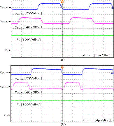
Fig. 2. Experimental waveforms for the gate signals and output voltage according to the operation mode. (a) PSFB series-resonant converter mode when Vd = 350 V. (b) Active-clamp step-up converter when Vd = 250 V.


Fig. 3. Experimental waveforms for soft switching in the PSFB series resonant converter mode. (a) ZVS turn-on of S1 . (b) ZVS turn-on and ZCS turn-off of S2


.

Fig. 4. Experimental waveforms for the current stress when Vd = 350 V. (a) Conventional PSFB series-resonant converter. (b) Proposed converter.


Fig. 5. Experimental waveforms for the input voltage Vd and output voltage Vo in the transition-state.

CONCLUSION:

The novel hybrid-type full-bridge dc/dc converter with high efficiency has been introduced and verified by the analysis and experimental results. By using the hybrid control scheme with the simple circuit structure, the proposed converter has both the step-down and step-up functions, which ensure to cover the wide input range. Under the normal input range, the proposed converter achieves high efficiency by providing soft switching technique to all the switches and rectifier diodes, and reducing the current stress. When the input is lower than the normal input range, the proposed converter provides the step-up function by using the active-clamp circuit and voltage doubler, which extends the operation range. To confirm the validity of the proposed converter, 1 kW prototype was built and tested. Under the normal input range, the conversion efficiency is over 96% at full-load condition, and the input range from 250 to 350 V is guaranteed. Thus, the proposed converter has many advantages such as high efficiency and wide input range.

REFERENCES:

[1] J. A. Sabat´e, V. Vlatkovic, R. B. Ridley, F. C. Lee, and B. H. Cho, “Design considerations for high-voltage high-power full-bridge zero-voltage switching PWM converter,” in Proc. Appl. Power Electron. Conf., 1990, pp. 275–284.
[2] I. O. Lee and G. W. Moon, “Phase-shifted PWM converter with a wide ZVS range and reduced circulating current,” IEEE Trans. Power Electron., vol. 28, no. 2, pp. 908–919, Feb. 2013.
[3] Y. S. Shin, S. S. Hong, D. J. Kim, D. S. Oh, and S. K. Han, “A new changeable full bridge dc/dc converter for wide input voltage range,” in Proc. 8th Int. Conf. Power Electron. ECCE Asia, May 2011, pp. 2328–2335.
[4] P. K. Jain, W., Kang, H. Soin, and Y. Xi, “Analysis and design considerations of a load and line independent zero voltage switching full bridge dc/dc converter topology,” IEEE Trans. Power Electron., vol. 17, no. 5, pp. 649–657, Sep. 2002.

[5] I. O. Lee and G. W. Moon, “Soft-switching DC/DC converter with a full ZVS range and reduced output filter for high-voltage application,” IEEE Trans. Power Electron., vol. 28, no. 1, pp. 112–122, Jan. 2013.

Saturday, 1 April 2017

A Hybrid-STATCOM with Wide Compensation Range and Low DC-Link Voltage


ABSTRACT:
This paper proposes a hybrid static synchronous compensator (hybrid-STATCOM) in a three-phase power transmission system that has a wide compensation range and low DC-link voltage. Because of these prominent characteristics, the system costs can be greatly reduced. In this paper, the circuit configuration of hybrid-STATCOM is introduced first. Its V-I characteristic is then analyzed, discussed, and compared with traditional STATCOM and capacitive-coupled STATCOM (C-STATCOM). The system parameter design is then proposed on the basis of consideration of the reactive power compensation range and avoidance of the potential resonance problem. After that, a control strategy for hybrid-STATCOM is proposed to allow operation under different voltage and current conditions, such as unbalanced current, voltage dip, and voltage fault. Finally, simulation and experimental results are provided to verify the wide compensation range and low DC-link voltage characteristics and the good dynamic performance of the proposed hybrid-STATCOM.
KEYWORDS:

1.      Capacitive-coupled static synchronous compensator (C-STATCOM)
2.       Hybrid static synchronous compensator (hybrid-STATCOM)
3.       Static synchronous compensator (STATCOM)
4.       Wide compensation range  
5.      Low DC-link voltage

SOFTWARE: MATLAB/SIMULINK

BLOCK DIAGRAM:


Fig. 1. Circuit configuration of the hybrid-STATCOM.


EXPECTED SIMULATION RESULTS:


Fig. 2. Dynamic compensation waveforms of load voltage, source current, and load and source reactive powers by applying hybrid-STATCOM under different loadings cases.


Fig. 3 Dynamic compensation waveforms of vx and isx by applying hybrid-STATCOM under (a) inductive load, (b) capacitive load and (c) changing from capacitive load to inductive load.


Fig. 4. Dynamic compensation waveforms of vx and isx by applying hybrid-STATCOM under unbalanced loads.


Fig. 5. Dynamic compensation waveforms of vx and isx by applying hybrid-STATCOM under voltage fault condition.


Fig. 6. Dynamic compensation waveforms of vx and isx by applying hybrid-STATCOM during voltage dip.

CONCLUSION:

In this paper, a hybrid-STATCOM in three-phase power system is proposed and discussed as a cost-effective reactive power compensator for medium voltage level application. The system configuration and V-I characteristic of the hybrid-STATCOM are analyzed, discussed, and compared with traditional STATCOM and C-STATCOM. In addition, its parameter design method is proposed on the basis of consideration of the reactive power compensation range and prevention of a potential resonance problem. Moreover, the control strategy of the hybrid-STATCOM is developed under different voltage and current conditions. Finally, the wide compensation range and low DC-link voltage characteristics with good dynamic performance of the hybrid-STATCOM are proved by both simulation and experimental results.

REFERENCES:
[1] J. Dixon, L. Moran, J. Rodriguez, and R. Domke, “Reactive power compensation technologies: State-of-the-art review,” Proc. IEEE, vol. 93, no. 12, pp. 2144–2164, Dec. 2005.
[2] L. Gyugyi, R. A. Otto, and T. H. Putman, “Principles and applications of static thyristor-controlled shunt compensators,” IEEE Trans. Power App. Syst., vol. PAS-97, no. 5, pp. 1935–1945, Sep./Oct. 1978.
[3] T. J. Dionise, “Assessing the performance of a static var compensator for an electric arc furnace,” IEEE Trans. Ind. Appl., vol. 50, no. 3, pp. 1619–1629, Jun. 2014.a
[4] F. Z. Peng and J. S. Lai, “Generalized instantaneous reactive power theory for three-phase power systems,” IEEE Trans. Instrum. Meas., vol. 45, no. 1, pp. 293–297, Feb. 1996.

[5] L. K. Haw, M. S. Dahidah, and H. A. F. Almurib, “A new reactive current reference algorithm for the STATCOM system based on cascaded multilevel inverters,” IEEE Trans. Power Electron., vol. 30, no. 7, pp. 3577–3588, Jul. 2015.

Wednesday, 29 March 2017

A Novel Power Factor Correction Technique/or a Boost Converter


ABSTRACT:
The paper evolves a mechanism for improving the input power factor of an AC-DC-DC conversion system. It involves the process of shaping the input current wave to phase align with the input supply through a process of error compensation. The methodology includes cohesive formulation to arrive at nearly unity power factor and enjoy the etiquettes of output voltage regulation. The theory assuages to subscribe the benefits for the entire range of operating loads. It eliminates the use of passive components and fortifies the principles of pulse width modulation (PWM) for realizing the change in duty cycle. The MA TLAB based simulation results arbitrate the viability of the proposed approach and exhibit its suitability for use in real world applications.

KEYWORDS:
1.      Ac-dc converter
2.      Power factor
3.      THD
4.      Voltage regulation

SOFTWARE: MATLAB/SIMULINK


CIRCUIT DIAGRAM:

Figure 1. Power Factor Correction Control of Boost Converter


EXPECTED SIMULATION RESULTS:


Figure 2. Steady State Input AC Voltage and Input AC Current Waveform


Figure 3. Steady State Rectified DC Voltage and Rectified DC Current Waveform


Figure 4. Steady State Regulated DC Output Voltage and Regulated DC Output Current Waveform

Figure 5. Power Factor Measurement of the Proposed Power Factor Correction Boost Converter


Figure 6. FFT Spectrum of the AC input current of Proposed Power Factor Correction Boost Converter

Figure 7. Transient response of Input AC Voltage and Input AC Current Waveform

Figure 8. Transient Response of Rectified DC Voltage and Rectified DC Current Waveform


Figure 9. Transient Response of Regulated DC Output Voltage and Regulated DC Output Current Waveform


Figure 10. Power Factor Measurement of the Proposed Power Factor Correction Boost Converter at transient condition

CONCLUSION:
A single stage power factor correction strategy has been proposed for full bridge diode rectifier fed boost converter to support a 400W, lA DC load. The suitability of boost converter for power factor correction has been illustrated by the elimination of input capacitor filter and low output ripple factor. The formulated control design has been effectively orchestrated to correct the power factor in addition providing good voltage regulation. The transient performance has been portrayed to up-heave the strength of the control structure with an adequate output regulation and effective harmonic elimination. The control plan has been nurtured to standardize the THD level of the system that prevents the adverse effects of harmonics being injected in the grid. The exclusion of additional passive components and interleaving configuration has been fostered to reduce the size thus making it more adaptive to low cost compact electronic applications with high standards .

REFERENCES:
[1] M. Milanovic, F . Mihalic, K. Jezernik and U. Milutinovic," Single phase unity power factor correction circuits with coupled inductance," Power Electronics Specialists Conference, 1992, vol.2, pp. l077-1082.
[2] M. Orabi and T Ninomiya, "Novel nonlinear representation for two stage power-factor-correction converter instability," IEEE International Symposium on Industrial Electronics, 2003, voU, pp- 270-274.
[3] Yu Hung, Dan Chen, Chun-Shih Huang and Fu-Sheng Tsai, "Pulse-skipping power factor correction control schemes for ACIDC power converters," Fourth International Conference on Power Engineering, Energy and Electrical Drives (POWERENG), 2013, pp-I087-1092.
[4] Lu, D.D. -C, H.H.-C. lu, V. Pjevalica, "A Single-Stage AC/DC Converter With High Power Factor, Regulated Bus Voltage, and Output Voltage," Power Electronics, IEEE Transactions on, vo1.23, issue. I, pp. 218-228, Jan. 2008.

[5] M. Narimani and G. Moschopoulos, "A New Single-Phase SingleStage Three-Level Power Factor Correction AC-DC Converter," Power Electronics, IEEE Transactions on , vol.27, issue.6, pp. 2888- 2899, June. 2012.