asokatechnologies@gmail.com 09347143789/09949240245

Search This Blog

Sunday, 14 May 2017

Naturally Clamped Zero Current Commutated Soft-switching Current-fed Push-Pull DC/DC Converter: Analysis, Design, and Experimental Results

ABSTRACT:
The proposed converter has the following features: 1) zero current commutation (ZCC) and natural voltage clamping (NVC) eliminate the need for active-clamp circuits or passive snubbers required to absorb surge voltage in conventional current-fed topologies; 2) Switching losses are reduced significantly owing to zero-current switching (ZCS) of primary side devices and zero-voltage switching (ZVS) of secondary side devices. Turn-on switching transition loss of primary devices is also negligible. 3) Soft-switching and NVC are inherent and load independent. 4) The voltage across primary side device is independent of duty cycle with varying input voltage and output power and clamped at rather low reflected output voltage enabling the use of low voltage semiconductor devices. These merits make the converter good candidate for interfacing low voltage dc bus with high voltage dc bus for higher current applications. Steady state, analysis, design, simulation and experimental results are presented.

KEYWORDS:
1.      Current-fed converter
2.       DC/DC converter
3.      Natural clamping
4.       Soft-switching
5.       Zero-current commutation

SOFTWARE: MATLAB/SIMULINK

BLOCK DIAGRAM:
Fig. 1. Diagram of a FCV propulsion system.


CIRCUIT DIAGRAM:
Fig.2. Proposed ZCS current-fed push-pull dc/dc converter.

  
  EXPECTED SIMULATION RESULTS:

Fig. 3. Operating waveforms of proposed ZCS current-fed push-pull converter
in the buck mode.

 Fig. 4. Simulation results for output power of 250W at 300V. (a) Current through input inductor iL and voltage VAB. (b) Primary switches currents iS1 and iS2 and secondary switches currents iS3 and iS4.


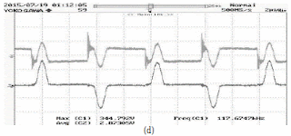
Fig. 5. Experimental results for output power of 250W at 300V(x-axis: 2μs/div): (a) Boost inductor current iL (5A/div), (b) Voltage vAB (100V/div) and voltage across secondary of transformer vsec (500 V/div), (c-d) Gate-to-source voltage Vgs (10V/div) and drain-to-source voltage Vds (50V/div) across the primary side MOSFETs and currents through them (10A/div). (e-f) Gate-to-source voltage Vgs (10V/div) and drain-to-source voltage Vds (200V/div) across the secondary side MOSFETs and currents through them (2A/div).


Fig. 6. Experimental results for output power of 100W at 300V(x-axis: 2μs/div): (a) Boost inductor current iL (5A/div), (b) Voltage vAB (100V/div) and voltage across secondary of transformer vsec (500 V/div), (c-d) Gate-to-source voltage Vgs (10V/div) and drain-to-source voltage Vds (50V/div) across the primary side MOSFETs and currents through them (10A/div). (e-f) Gate-to-source voltage Vgs (10V/div) and drain-to-source voltage Vds (200V/div) across the secondary side MOSFETs and currents through them (2A/div).


CONCLUSION:
This paper presents a novel soft-switching snubberless bidirectional current-fed isolated push-pull dc/dc converter for application of the ESS in FCVs. A novel secondary side modulation method is proposed to eliminate the problem of voltage spike across the semiconductor devices at turn-off. The above claimed ZCC and NVC of primary devices without any snubber are demonstrated and confirmed by the simulation and experimental results. ZCS of primary side devices and ZVS of secondary side devices are achieved, which reduces the switching losses significantly. Soft-switching is inherent and is maintained independent of load. Once ZCC, NVC, and soft-switching are designed to be obtained at rated power, it is guaranteed to happen at reduced load unlike voltage-fed converters. Turn-on switching transition loss of primary devices is also shown to be negligible. Hence maintaining soft-switching of all devices substantially reduces the switching loss and allows higher switching frequency operation for the converter to achieve a more compact and higher power density system. Proposed secondary modulation achieves natural commutation of primary devices and clamps the voltage across them at low voltage (reflected output voltage) independent of duty cycle. It therefore eliminates requirement of active-clamp or passive snubber. Usage of low voltage devices results in low conduction losses in primary devices, which is significant due to higher currents on primary side. The proposed modulation method is simple and easy to implement. These merits make the converter promising for interfacing low voltage dc bus with high voltage dc bus for higher current applications such as FCVs, front-end dc/dc power conversion for renewable (fuel cells/PV) inverters, UPS, microgrid, V2G, and energy storage. The specifications are taken for FCV but the proposed modulation, design, and the demonstrated results are suitable for any general application of current-fed converter (high step-up). Similar merits and performance will be achieved.

REFERENCES:
[1] A. Khaligh and Z. Li, “Battery, ultracapacitor, fuel cell, and hybrid energy storage systems for electric, hybrid electric, fuel cell, and plug-in hybrid electric vehicles: State of the art”, IEEE Trans. on Vehicular Technology, vol. 59, no. 6, pp. 2806- 2814, Oct. 2009.
[2] A. Emadi, and S. S. Williamson, “Fuel cell vehicles: opportunities and challenges,” in Proc. IEEE PES, 2004, pp. 1640-1645.
[3] K. Rajashekhara, “Power conversion and control strategies for fuel cell vehicles,” in Proc. IEEE IECON, 2003, pp. 2865-2870.
[4] A. Emadi, S. S. Williamson, and A. Khaligh, “Power electronics intensive solutions for advanced electric, hybrid electric, and fuel cell vehicular power systems,” IEEE Trans. Power Electron., vol. 21, no. 3, pp. 567–577, May. 2006.
[5] A. Emadi, K. Rajashekara, S. S. Williamson, and S. M. Lukic, “Topological overview of hybrid electric and fuel cell vehicular power system architectures and configurations” IEEE Trans. on Vehicular

Technology, vol. 54, no. 3, pp. 763–770, May. 2005.

Extended Range ZVS Active-Clamped Current-Fed Full-Bridge Isolated DC/DC Converter for Fuel Cell Applications: Analysis, Design, and Experimental Results


ABSTRACT:
This paper presents analysis and design of zero voltage switching (ZVS) active-clamped current-fed full-bridge isolated dc/dc converter for fuel cell applications. The designed converter maintains ZVS of all switches from full load down to very light load condition over wide input voltage variation. Detailed operation, analysis, design, simulation, and experimental results for the proposed design are presented. The additional auxiliary active clamping circuit absorbs the turn-off voltage spike limiting the peak voltage across the devices allowing the selection and use of low-voltage devices with low on-state resistance. In addition, it also assists in achieving ZVS of semiconductor devices. The converter utilizes the energy stored in the transformer leakage inductance aided by its magnetizing inductance to maintain ZVS. ZVS range depends upon the design, in particular the ratio of leakage and magnetizing inductances of the transformer. Rectifier diodes operate with zero-current switching. An experimental converter prototype rated at 500 W has been designed, built, and tested in the laboratory to verify the analysis, design, and performance for wide variations in input voltage and load.
KEYWORDS:
1.      Fuel cells
2.      High-frequency (HF) dc/dc converter
3.      Renewable energy systems
4.      Zero voltage switching (ZVS)

SOFTWARE: MATLAB/SIMULINK

CIRCUIT DIAGRAM:


Fig. 1. Active-clamped ZVS current-fed full-bridge dc-dc converter.

EXPECTED SIMULATION RESULTS:


Fig. 2. Simulation waveforms at Vin = 22 V and full load: (a) voltage vAB, leakage inductance current ilk, and magnetizing inductance current iLm (b) main switches’ currents iS1 and iS2, auxiliary switch’s current iSax and voltage across auxiliary capacitor VCa.


Fig. 3. Simulation waveforms at Vin = 41 V and 10% load: (a) voltage vAB, leakage inductance current ilk, and magnetizing inductance current iLm (b) main switches’ currents iS1 and iS2, auxiliary switch’s current iSax and voltage across auxiliary capacitor VCa.


Fig. 4. Experimental waveforms at Vin = 22 V and full load: (a) Voltage vAB (100 V/div) and leakage inductance current ilk (50 A/div), (b) main switch voltage vDS (50 V/div) and gate voltage vGS (10 V/div), (c) auxiliary switch voltage vDS (50 V/div) and gate voltage vGS (20 V/div), (d) main switch current iS1 (20 A/div), (e) auxiliary switch current iSax (20 A/div) and (f) magnetizing inductance current iLm (0.5 A/div).


Fig. 5. Experimental waveforms at Vin = 41 V and full load: (a) Voltage vAB (50 V/div) and leakage inductance current ilk (50 A/div), (b) main switch voltage vDS (50 V/div) and gate voltage vGS (10 V/div), (c) auxiliary switch voltage vDS (50 V/div) and gate voltage vGS (20 V/div), (d) main switch current iS1 (20 A/div), (e) auxiliary switch current iSax (10 A/div) and (f) magnetizing inductance current iLm (1 A/div).


Fig. 6. Experimental waveforms at Vin = 22 V and 20% load: (a) Voltage vAB (50 V/div) and leakage inductance current ilk (10 A/div), (b) main switch voltage vDS (50 V/div), gate voltage vGS (20 V/div) and current iS1 (10 A/div), (c) auxiliary switch voltage vDS (50 V/div) and gate voltage Vgs (10 V/div), (d) auxiliary switch current iSax (5 A/div) and (e) magnetizing inductance current iLm (0.5 A/div).


Fig. 7. Experimental waveforms at Vin = 41 V and 10% load. (a) Voltage vAB (50 V/div) and leakage inductance current ilk (10 A/div), (b) main  switch voltage vDS (50 V/div) and gate voltage vGS (10 V/div), (c) auxiliary  switch voltage vDS (50 V/div) and gate voltage vGS (10 V/div), (d) main switch current iS1 (10 A/div), (e) auxiliary switch current iSax (5 A/div) and (f) magnetizing inductance current iLm (1 A/div).

CONCLUSION:
 To achieve ZVS for wide source voltage variation and varying output power/load while maintaining high efficiency has been a challenge, particularly for low-voltage higher current input applications. A ZVS active-clamped current-fed full bridge isolated converter has been restudied in this paper. The magnetizing inductance increases the leakage inductance current value at light load and therefore the energy stored in leakage inductance to maintain ZVS of main switches as well as auxiliary switch.
Detailed steady-state operation and analysis of current-fed full-bridge converter have been presented. Design to attain soft switching over an extended range of input voltage and load i.e., output power has been presented. Simulation results using PSIM 9.0.4 have been presented. An  experimental prototype of. the converter rated at 500Whas been designed, built, and tested for variations in input voltage and load in order to validate the analysis. Experimental results verify the accuracy of the analysis and show that the proposed configuration is able to maintain ZVS of all switches over a wide range of load and input voltage variation due to the variation in fuel flow and stack temperature. Theoretically, the converter is able to maintain ZVS till 20% load at 22 V and 5% load 41 V.
In a practical fuel cell application, when the load current drops due to reduced fuel flow, the light or reduced power below rated power is transferred at higher fuel cell voltage. It can be clearly seen and understood also from the fuel cell V I characteristic. If the load current or power is around 10% of the rated power, then the fuel cell stack voltage increases nearly to 41 V. Hence, the possibility of the condition Vin = 22 V at 10% load is only during transition period when load is suddenly changed from full load to 10% due to fuel flow adjustment. Hence, it is justifiable to have ZVS range of 20% load at low input voltage and below 10% at higher input voltage will cover the operating range at steady state. Rated converter efficiency of 94% is obtained for the developed lab prototype rated at 500 W. The converter has limitation that duty cycle of the main switch should be greater than 50%.

REFERENCES:
[1] S. Jain and V. Agarwal, “An integrated hybrid power supply for distributed generation applications fed by nonconventional energy sources,” IEEE Trans. Energy Convers., vol. 23, no. 2, pp. 622–631, Jun. 2008.
[2] Y. Lembeye, V. D. Bang, G. Lefevre, and J. P. Ferrieux, “Novel half-bridge inductive dc-dc isolated converters for fuel cell applications,” IEEE Trans. Energy Convers., vol. 24, no. 1, pp. 203–210, Mar. 2009.
[3] J. Mazumdar, I. Batarseh, N. Kutkut, and O. Demirci, “High frequency low cost dc-ac inverter design with fuel cell source home applications,” in Conf. Rec. IEEE IAS Annu. Meeting, Oct. 2002, vol. 2, pp. 789–794.
[4] J. Wang, F. Z. Peng, J. Anderson, A. Joseph, and R. Buffenbarger, “Low cost fuel cell converter system for residential power generation,” IEEE Trans. Power Electron., vol. 19, no. 5, pp. 1315–1322, Sep. 2004.
[5] R. Gopinath, S. Kim, J.-H. Hahn, P. N. Enjeti, M. B. Yeary, and J. W. Howze, “Development of a low cost fuel cell inverter system with DSP control,” IEEE Trans. Power Electron., vol. 19, no. 5, pp. 1256–1262, Sep. 2004.


Saturday, 13 May 2017

Design and Performance of a Bidirectional Isolated DC–DC Converter for a Battery Energy Storage System


ABSTRACT:
This paper describes the design and performance of a 6-kW, full-bridge, bidirectional isolated dc–dc converter using a 20-kHz transformer for a 53.2-V, 2-kWh lithium-ion (Li-ion) battery energy storage system. The dc voltage at the high-voltage side is controlled from 305 to 355 V, as the battery voltage at the low voltage side (LVS) varies from 50 to 59 V. The maximal efficiency of the dc–dc converter is measured to be 96.0% during battery charging, and 96.9% during battery discharging. Moreover, this paper analyzes the effect of unavoidable dc-bias currents on the magnetic-flux saturation of the transformer. Finally, it provides the dc–dc converter loss breakdown with more focus on the LVS converter.

KEYWORDS:
1.      Bidirectional isolated dc–dc converters
2.      Dc-bias currents
3.      Energy storage systems
4.      Lithium-ion (Li-ion) battery

SOFTWARE: MATLAB/SIMULINK

CIRCUIT DIAGRAM:


Fig. 1. Li-ion battery bank of 53.2 V, 40 A·h connected to the 6-kW bidirectional isolated dc–dc converter, where LS is the background system impedance (<1%). LAC = 280 μH (1.3%), LF = 44μH (0.2%), RF = 0.2Ω (3%), and CF = 150 μF (33%) on a three-phase 200 V, 6-kW, and 50-Hz base.


 EXPECTED SIMULATION RESULTS:


Fig. 2. Experimental waveforms with dc-voltage control at the HVS. (a) Charging mode at PB = 5.9 kW (VD1 = 355 V). (b) Discharging mode at PB = 5.9 kW (VD1 = 305 V).


Fig. 3. Waveforms of vD1, vB , and iB . (a) Battery charging at PB = 5.9 kW.
(b) Battery discharging at PB = 5.9 kW.

Fig. 4. Drain–source and gate–source voltages of a leg in bridge 2 at PB =
5.9 kW, VD1 = 355 V, and VB = 59V


Fig. 5. Effects of the RC-snubber on a MOSFET in bridge 2 during battery charging at PB = 5.9 kW. (a) Drain–source voltage and RC-snubber current. (b) Time-expanded waveform of vDS and iRC .

CONCLUSION:
This paper has presented the experimental results from the combination of a 53.2-V, 40-A·h Li-ion battery bank with a single-phase full-bridge bidirectional isolated dc–dc converter. The results have verified the proper operation of the Li-ion battery energy storage system. Discussions focusing on magnetic flux saturation due to unavoidable dc-bias currents at the high voltage and LVSs have been carried out. The transformer with an air-gap length of 1 mm has been shown experimentally to be robust against magnetic-flux saturation, even in the worst cases. The bidirectional isolated dc–dc converter exhibits high efficiency in the low-voltage and high-current operation. From the estimation of loss distribution in the dc–dc converter, a large portion of the loss at the rated power is caused by the turn off switching loss at the LVS. One of the best methods of improving the efficiency of the dc–dc converter is to operate it at a lower switching frequency. However, this method is accompanied by acoustic noise generation and a bulky transformer.

REFERENCES:
[1] New Energy and Industrial Technology Development Organization (NEDO). (2008). Global warming counter measures: Japanese technologies for energy savings/GHG (greenhouse gases) emissions reduction (Revised ed.), [Online]. Available: http://www.nedo.go.jp
[2] S. C. Smith, P. K. Sen, and B. Kroposki, “Advancement of energy storage devices and applications in electrical power system,” in Proc. IEEE Power Energy Soc. General Meeting, Jul. 2008, pp. 1–8.
[3] P. F. Ribeiro, B. K. Johnson, M. L. Crow, A. Arsoy, and Y. Liu, “Energy storage systems for advanced power applications,” Proc. IEEE, vol. 89, no. 12, pp. 1744–1756, Dec. 2001.
[4] R.W. A. A. De Doncker, D. M. Divan, and M. H. Kheraluwala, “A threephase soft-switched high-power-density dc/dc converter for high power applications,” IEEE Trans. Ind. Appl., vol. 27, no. 1, pp. 63–73, Feb. 1991.
[5] M. H. Kheraluwala, R. W. Gascoigne, D. M. Divan, and E. D. Baumann, “Performance characterization of a high-power dual active bridge dc-todc converter,” IEEE Trans. Ind. Appl., vol. 28, no. 6, pp. 1294–1301, Nov./Dec. 1992.


Parasitics Assisted Soft-switching and Naturally Commutated Current-fed Bidirectional Push-pull Voltage Doubler


ABSTRACT:
A snubberless current-fed push-pull dc/dc voltage doubler is proposed with zero voltage switching (ZVS) turn-on of low voltage current-fed devices by using the parasitic resonance between the drain-source capacitance of MOSFETs and the leakage inductance of the high frequency transformer. \Secondary modulation helps reduce switching losses further by obtaining zero current switching (ZCS) turn-off of primary devices and ZVS turn-on of secondary devices. Realizing ZCS of current-fed devices introduces natural zero current commutation and eliminates the traditional requirement of active-clamp or passive snubbers in current-fed topologies. Push-pull topology has low device and driver requirement. Voltage doubler offers 2x voltage gain reducing the device count by half on secondary that simplifies the transformer and control design and efficiently reduce the low frequency dc current harmonics. The proposed topology with novel modulation is suitable for interfacing energy storage and/or fuel cell stack with dc bus in FCVs or as frontend dc/dc converter in fuel cell inverters or connecting fuel cells to dc grid. Steady-state operation and analysis of proposed topology with proposed modulation has been studied. Design of a 1kW prototype is explained. Simulation results using PSIM 9.3 and experimental results of a 1 kW prototype have been demonstrated to verify the operation, proposed mathematical analysis, design, and the proposed claims.


 KEYWORDS:
1.      Current-fed converter
2.      Push-pull
3.      Natural commutation
4.      Soft-switching

SOFTWARE: MATLAB/SIMULINK

BLOCK DIAGRAM:


 Fig.1. Architecture of a dc microgrid


Fig. 2. Architecture of a fuel cell car.


EXPECTED SIMULATION RESULTS:


Fig.2. Simulation results: (a) Gating signal of switch S1, current through switch S1, voltage across switch S1,(b) Gating signal of switch S2, current through switch S2, voltage across switch S2, (c) Current through boost inductor L, Current through series leakage inductance, Llk1, Current through series leakage inductance, Llk2, (d) Current through secondary devices S3 and S4, (e) Voltage Vab, output voltage Vo,Voltage across Llk1


Fig. 3. Experimental results: (a) Gating signal of switch S1, Vgs1, current through switch S1, Is1, drain-source voltage across switch S1, Vds1, (b) Current through boost inductor L, current through series leakage inductance, Llk1, (c) Current through secondary device S3, Is3, Gating pulse of S3, Vgs3, drain source voltage across switch S3, Vds3, (d) Voltage across leakage inductor Vlk1, voltage across transformer primary, Vab,


  CONCLUSION:
A truly snubberless current-fed push-pull dc/dc converter is proposed with zero current commutation and natural device voltage clamping. Push-pull configuration and voltage doubler circuit reduces the active device and driver count. It leads to a simple control design and implementation. Voltage doubler improves the gain by 2x and reduce transformer size. Traditionally, current-fed converters are hard-switching with device voltage spike at turn-off and require snubber circuits. In this paper, an innovative modulation is proposed to utilize circuit parasitics and introduce soft-switching of all devices. Zero current commutation and device voltage clamping are obtained without additional snubber making it a truly snubberless topology. The proposed modulation solves the classical problem in current-fed converters and makes a novel contribution. Furthermore, the proposed converter topology can efficiently eliminate the low frequency current ripples on the source (fuel cell stack) side. Low frequency dc current harmonics coming from power electronics have a negative impact on the lifetime and the performance of fuel cell power generation systems. The elimination of such low frequency current ripples may also simplify the control of fuel cell system ancillaries, such as air compressor. Thus, it is suitable for low voltage high current applications requiring high voltage gain, low ripple dc current, and precise operating point control. Major applications include interfacing energy storage with dc link in FCVs due to bidirectional nature and also as a front end dc-dc converter in case of fuel cell inverters. Switching losses are reduced significantly owing to soft-switching of all the devices. Synchronous rectification may be employed to obtain high efficiency. Steady state operation, analysis and circuit design have been explained in detail. Simulation results are presented to verify the concept and experimental results are demonstrated to show the performance and the claims.

REFERENCES:
[1] F. A. Farret, M. G. Simoes, “Integration of Alternative Sources of Energy,” 1st ed. New Jersey: Wiley, 2006.
[2] A. Khaligh and Z. Li, “Battery, ultracapacitor, fuel cell, and hybrid energy storage systems for electric, hybrid electric, fuel cell, and plugin hybrid electric vehicles: State of the art,” IEEE Trans. Veh. Technol., vol. 59, no. 6, pp. 2806–2814, Oct. 2009.
[3] A. Emadi and S. S. Williamson, “Fuel cell vehicles: Opportunities and challenges,” in Proc. IEEE Power Eng. Soc., 2004, pp. 1640–1645.
[4] K. Rajashekhara, “Power conversion and control strategies for fuel cell vehicles,” in Proc. IEEE Annu. Conf. Ind. Electron. Soc., 2003, pp. 2865– 2870.

[5] A. Emadi, S. S. Williamson, and A. Khaligh, “Power electronics intensive solutions for advanced electric, hybrid electric, and fuel cell vehicular power systems,” IEEE Trans. Power Electron., vol. 21, no. 3, pp. 567– 577, May 2006.