Naturally Clamped Zero Current
Commutated Soft-switching Current-fed Push-Pull DC/DC Converter: Analysis,
Design, and Experimental Results
ABSTRACT:
The proposed converter has the following features:
1) zero current commutation (ZCC) and natural voltage clamping (NVC) eliminate
the need for active-clamp circuits or passive snubbers required to absorb surge
voltage in conventional current-fed topologies; 2) Switching losses are reduced
significantly owing to zero-current switching (ZCS) of primary side devices and
zero-voltage switching (ZVS) of secondary side devices. Turn-on switching
transition loss of primary devices is also negligible. 3) Soft-switching and
NVC are inherent and load independent. 4) The voltage across primary side device
is independent of duty cycle with varying input voltage and output power and
clamped at rather low reflected output voltage enabling the use of low voltage semiconductor
devices. These merits make the converter good candidate for interfacing low
voltage dc bus with high voltage dc bus for higher current applications. Steady
state, analysis, design, simulation and experimental results are presented.
KEYWORDS:
1. Current-fed
converter
2. DC/DC converter
3. Natural clamping
4. Soft-switching
5. Zero-current commutation
SOFTWARE: MATLAB/SIMULINK
BLOCK DIAGRAM:

Fig. 1. Diagram of a FCV propulsion
system.
CIRCUIT DIAGRAM:

Fig.2.
Proposed ZCS current-fed push-pull dc/dc converter.
EXPECTED SIMULATION RESULTS:

Fig. 3. Operating waveforms of proposed
ZCS current-fed push-pull converter
in the buck mode.

Fig.
4. Simulation results for output power of 250W at 300V. (a) Current through
input inductor iL and voltage VAB. (b)
Primary switches currents iS1 and iS2
and secondary switches currents iS3 and iS4.


Fig.
5. Experimental results for output power of 250W at 300V(x-axis: 2μs/div): (a)
Boost inductor current iL (5A/div), (b) Voltage vAB
(100V/div) and voltage across secondary of transformer vsec
(500 V/div), (c-d) Gate-to-source voltage Vgs (10V/div) and
drain-to-source voltage Vds (50V/div) across the primary side
MOSFETs and currents through them (10A/div). (e-f) Gate-to-source voltage Vgs
(10V/div) and drain-to-source voltage Vds (200V/div) across
the secondary side MOSFETs and currents through them (2A/div).
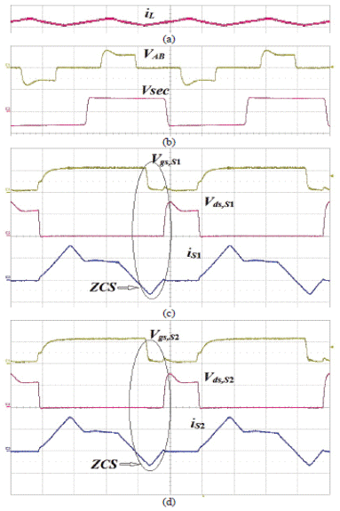

Fig.
6. Experimental results for output power of 100W at 300V(x-axis: 2μs/div): (a)
Boost inductor current iL (5A/div), (b) Voltage vAB (100V/div)
and voltage across secondary of transformer vsec (500 V/div), (c-d)
Gate-to-source voltage Vgs (10V/div) and drain-to-source voltage Vds (50V/div)
across the primary side MOSFETs and currents through them (10A/div). (e-f) Gate-to-source
voltage Vgs (10V/div) and drain-to-source voltage Vds (200V/div) across
the secondary side MOSFETs and currents through them (2A/div).
CONCLUSION:
This
paper presents a novel soft-switching snubberless bidirectional current-fed
isolated push-pull dc/dc converter for application of the ESS in FCVs. A novel
secondary side modulation method is proposed to eliminate the problem of voltage
spike across the semiconductor devices at turn-off. The above claimed ZCC and
NVC of primary devices without any snubber are demonstrated and confirmed by
the simulation and experimental results. ZCS of primary side devices and ZVS of
secondary side devices are achieved, which reduces the switching losses
significantly. Soft-switching is inherent and is maintained independent of
load. Once ZCC, NVC, and soft-switching are designed to be obtained at rated
power, it is guaranteed to happen at reduced load unlike voltage-fed converters.
Turn-on switching transition loss of primary devices is also shown to be
negligible. Hence maintaining soft-switching of all devices substantially
reduces the switching loss and allows higher switching frequency operation for
the converter to achieve a more compact and higher power density system.
Proposed secondary modulation achieves natural commutation of primary devices
and clamps the voltage across them at low voltage (reflected output voltage) independent
of duty cycle. It therefore eliminates requirement of active-clamp or passive
snubber. Usage of low voltage devices results in low conduction losses in
primary devices, which is significant due to higher currents on primary side.
The proposed modulation method is simple and easy to implement. These merits
make the converter promising for interfacing low voltage dc bus with high
voltage dc bus for higher current applications such as FCVs, front-end dc/dc
power conversion for renewable (fuel cells/PV) inverters, UPS, microgrid, V2G, and
energy storage. The specifications are taken for FCV but the proposed
modulation, design, and the demonstrated results are suitable for any general
application of current-fed converter (high step-up). Similar merits and
performance will be achieved.
REFERENCES:
[1]
A. Khaligh and Z. Li, “Battery, ultracapacitor, fuel cell, and hybrid energy storage
systems for electric, hybrid electric, fuel cell, and plug-in hybrid electric
vehicles: State of the art”, IEEE Trans. on Vehicular Technology, vol.
59, no. 6, pp. 2806- 2814, Oct. 2009.
[2]
A. Emadi, and S. S. Williamson, “Fuel cell vehicles: opportunities and challenges,”
in Proc. IEEE PES, 2004, pp. 1640-1645.
[3]
K. Rajashekhara, “Power conversion and control strategies for fuel cell vehicles,”
in Proc. IEEE IECON, 2003, pp. 2865-2870.
[4]
A. Emadi, S. S. Williamson, and A. Khaligh, “Power electronics intensive solutions
for advanced electric, hybrid electric, and fuel cell vehicular power systems,”
IEEE Trans. Power Electron., vol. 21, no. 3, pp. 567–577, May. 2006.
[5]
A. Emadi, K. Rajashekara, S. S. Williamson, and S. M. Lukic, “Topological
overview of hybrid electric and fuel cell vehicular power system architectures
and configurations” IEEE Trans. on Vehicular
Technology,
vol. 54, no. 3, pp. 763–770, May. 2005.