asokatechnologies@gmail.com 09347143789/09949240245

Search This Blog

Thursday, 29 June 2017

A Sensorless Power Reserve Control Strategy for Two-Stage Grid-Connected PV Systems

ABSTRACT
Due to the still increasing penetration of grid connected Photovoltaic (PV) systems, advanced active power control functionalities have been introduced in grid regulations. A power reserve control, where namely the active power from the PV panels is reserved during operation, is required for grid support. In this paper, a cost-effective solution to realize the power reserve for two-stage grid-connected PV systems is proposed. The proposed solution routinely employs a Maximum Power Point Tracking (MPPT) control to estimate the available PV power and a Constant Power Generation (CPG) control to achieve the power reserve. In this method, the solar irradiance and temperature measurements that have been used in conventional power reserve control schemes to estimate the available PV power are not required, and thereby being a sensorless approach with reduced cost. Experimental tests have been performed on a 3-kW two-stage single-phase grid-connected PV system, where the power reserve control is achieved upon demands.

KEYWORDS:
1.      Active power control
2.      Power reserve control
3.      Maximum power point tracking
4.      Constant power generation control
5.      PV systems
6.      Grid-connected power converters.

SOFTWARE: MATLAB/SIMULINK

BLOCK DIAGRAM:

Fig.1.System configuration and control structure of a two-stage grid connected
PV system with the Sensorless Power Reserve Control strategy.

EXPECTED EXPERIMENTAL RESULTS:


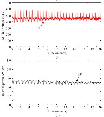
Fig. 2. Experimental results of the single-phase grid-connected PV system
with the proposed SPRC strategy during the steady-state operation (solar
irradiance level: 1000 W/m2; ambient temperature: 250C; available power
estimation rate: fAPE = 0.2 Hz), where the reference power reserve ∆P are
700 W, 500 W, and 300 W: (a) PV voltage vpv, (b) PV power Ppv and ac
power (Pac), (c) dc-link voltage vdc, and (d) reserved power ∆P.


Fig. 3. Experimental results of the single-phase grid-connected PV system
with the proposed SPRC strategy at the sampling rate of fAPE = 0.05 Hz
under a ramp-changing solar irradiance profile (ambient temperature: 250C),
where the reference power reserve ∆P is 500 W: (a) PV voltage vpv, (b)
PV power Ppv and ac power (Pac), (c) dc-link voltage vdc, and (d) reserved
power ∆P.


Fig. 4. Experimental results of the single-phase grid-connected PV system
with the proposed SPRC strategy at the sampling rate of fAPE = 0.2 Hz under
a ramp-changing solar irradiance profile (ambient temperature: 250C), where
the reference power reserve ∆P is 500 W: (a) PV voltage vpv, (b) PV power
Ppv and ac power (Pac), (c) dc-link voltage vdc, and (d) reserved power ∆P.


Fig. 5. Zoomed-in view of the results in Fig. 16: (a) PV voltage vpv, (b) PV
power Ppv and ac power (Pac), (c) dc-link voltage vdc, (d) reserved power P.

Fig. 6. Experimental result of the PV voltage vpv and the dc-link voltage
vdc with different available power estimation sampling rates fAPE.

CONCLUSION
A cost-effective sensorless power reserve control strategy for two-stage grid-connected PV systems has been proposed in this paper. The cost-effectiveness of the proposal lies in the sensorless estimation of the available PV power, which is achieved by routinely employing a fast MPPT operation. Then, the estimated available power is used for calculating the set-point to limit the extracted PV power with the CPG operation. At the grid-side, the stored energy in the dc-link is adaptively controlled to minimize the power fluctuation during the available PV power estimation process, where the excessed energy is temporarily stored in the dc-link. With the above coordinated control strategy, the power reserve control can be achieved as it has been verified experimentally. Design considerations for a high control performance and the operational boundary have also been discussed to assist the practical implementations.

REFERENCES
[1]   REN21, “Renewables 2016: Global Status Report (GRS),” 2016. [Online]. Available: http://www.ren21.net/.
[2]    Fraunhofer ISE, “Recent Facts about Photovoltaics in Germany,” April 22, 2016. [Online]. Available: http://www.pv-fakten.de/.
[3]   Solar Power Europe, “Global Market Outlook For Solar Power 2015 - 2019,” 2015. [Online]. Available: http://www.solarpowereurope.org/.
[4]   E. Reiter, K. Ardani, R. Margolis, and R. Edge, “Industry perspectives on advanced inverters for us solar photovoltaic systems: Grid benefits, deployment challenges, and emerging solutions,” National Renewable Energy Laboratory (NREL), Tech. Rep. No. NREL/TP-7A40-65063., 2015.

[5]   Y. Yang, P. Enjeti, F. Blaabjerg, and H. Wang, “Wide-scale adoption of photovoltaic energy: Grid code modifications are explored in the distribution grid,” IEEE Ind. Appl. Mag., vol. 21, no. 5, pp. 21–31, Sep. 2015..

A 2 kW, Single-Phase,7-Level Flying Capacitor Multilevel Inverter with an Active Energy Buffer

ABSTRACT
High efficiency and compact single-phase inverters are desirable in many applications such as solar energy harvesting and electric vehicle chargers. This paper presents a 2 kW, 60 Hz, 450 VDC to 240 VAC power inverter, designed and tested subject to the specifications of the Google/IEEE Little Box Challenge. The inverter features a 7-level flying capacitor multilevel converter, with low-voltage GaN switches operating at 120 kHz. The inverter also includes an active buffer for twice-line-frequency power pulsation decoupling, which reduces the required capacitance by a factor of eight compared to conventional passive decoupling capacitors, while maintaining an efficiency above 99%. The inverter prototype is a self-contained box that achieves a high power density of 216 W/in3 and a peak overall efficiency of 97.6% while meeting the constraints including input current ripple, load transient, thermal and FCC Class B EMC specifications.

KEYWORDS:
1.      Single-phase
2.      Inverter
3.      Flying-capacitor multilevel
4.      GaN.

SOFTWARE: MATLAB/SIMULINK

BLOCK DIAGRAM:

Fig. 1. Full system overview of the single-phase inverter.

EXPECTED EXPERIMENTAL RESULTS:

Fig. 2. Waveforms showing active energy buffer operation at 2kW. Voltage
ripple on VC3 counters the ripple on VC1 so that the bus voltage is constant.


Fig. 3. Waveforms showing the output voltage, output current and the
switching node voltage (VSW) of the 7-level inverter at full load.

Fig. 4. Capacitor voltages of the 7-level inverter during full load operation,
obtained using National Instruments data acquisition system (PXIe-1073).

Fig. 5. Energy buffer operation during a load step-down from 100% to 75%.
The input current ripple becomes within specifications after 80 ms.

Fig. 6. Inverter operation during a load step-down from 100% to 75%.

Fig. 7. Conducted EMI measurement at full power (2kW) from 150 kHz to
30 MHz, obtained using Tektronix RSA5126A real-time signal analyzer.

CONCLUSION
This paper has presented a 2 kW, 450 VDC to 240 VRMS single-phase inverter. The dc to ac conversion is accomplished through a 7-level flying-capacitor multilevel converter, with GaN transistors switching at 120 kHz, which is the highest switching frequency achieved to date for a 7-level implementation. The commutation loop in the FCML converter is identified, and a switching cell design is used to minimize loop inductance and reduce the drain-source voltage ringing. In addition, the multilevel inverter is complemented by a series stacked buffer converter for twice-line-frequency ripple compensation. The active energy buffer achieves a high efficiency of 99% while reducing the required capacitor volume by a factor of eight. The combined inverter prototype successfully demonstrated a 216 W/in3 power density with a rectangular volume of 9.26 in3. A peak overall efficiency of 97.6% is achieved, including the power losses from control and cooling fan. The prototype meets all the specifications of the Google/IEEE Little Box Challenge, such as the current ripple, the load transient, the EMC and case temperature requirement, showcasing the capability of the multilevel converter design and the series stacked active energy buffer.

REFERENCES
[1]   J. W. Kolar, U. Drofenik, J. Biela, M. L. Heldwein, H. Ertl, T. Friedli, and S. D. Round, “Pwm converter power density barriers,” in Power Conversion Conference - Nagoya, 2007. PCC ’07, pp. P–9–P–29, April 2007.
[2]   T. Meynard and H. Foch, “Multi-level conversion: high voltage choppers and voltage-source inverters,” in Power Electronics Specialists Conference, 1992. PESC ’92 Record., 23rd Annual IEEE, pp. 397–403 vol.1, Jun 1992.
[3]    S. Allebrod, R. Hamerski, and R. Marquardt, “New transformerless, scalable modular multilevel converters for hvdc-transmission,” in Power Electronics Specialists Conference, 2008. PESC 2008. IEEE, pp. 174– 179, June 2008.
[4]   A. Antonopoulos, L. A¨ ngquist, S. Norrga, K. Ilves, L. Harnefors, and H. P. Nee, “Modular multilevel converter ac motor drives with constant torque from zero to nominal speed,” IEEE Transactions on Industry Applications, vol. 50, pp. 1982–1993, May 2014.
[5]   S. Debnath, J. Qin, B. Bahrani, M. Saeedifard, and P. Barbosa, “Operation, control, and applications of the modular multilevel converter: A review,” IEEE Transactions on Power Electronics, vol. 30, pp. 37–53, Jan 2015.

.

A Frequency Adaptive Phase Shift Modulation Control Based LLC Series Resonant Converter for Wide Input Voltage Applications

 ABSTRACT
This paper presents an isolated LLC series resonant DC/DC converter with novel frequency adaptive phase shift modulation control, which suitable for wide input voltage (200-400V) applications. The proposed topology integrates two half-bridge in series on the primary side to reduce the switching stress to half of the input voltage. Unlike the conventional converter, this control strategy increases the voltage gain range with ZVS to all switches under all operating voltage and load variations. Adaptive frequency control is used to secure ZVS in the primary bridge with regards to load change. To do so, the voltage gain becomes independent of the loaded quality factor. In addition, the phase shift control is used to regulate the output voltage as constant under all possible inputs. The control of these two variables also significantly minimizes the circulating current, especially from the low voltage side, which increases the efficiency as compared to a conventional converter. Experimental results of a 1Kw prototype converter with 200-400V input and 48V output are presented to verify all theoretical analysis and characteristics.

KEYWORDS:
1.      LLC
2.      Resonant converter
3.      Frequency adaptive phase shift modulation control (FAPSM)
4.      Zero-Voltage-Switching (ZVS)
5.      Wide gain range.

SOFTWARE: MATLAB/SIMULINK

CIRCUIT DIAGRAM:

Fig. 1. Proposed LLC resonant converter.

EXPECTED SIMULATION RESULTS:


Fig. 2(a). Simulation waveforms of proposed converter under 400V input, 48V output and full load condition.

Fig. 2(b). Simulation waveforms of proposed converter under 200V input, 48V output and full load condition.

Fig. 2(c). Simulation waveforms of proposed converter under 400V input, 48V output and 20% load condition.

Fig. 2(d). Simulation waveforms of proposed converter under 200V input, 48V output and 20% load condition.

CONCLUSION
In this paper, a variable frequency phase shift modulation control for a DAB LLC resonant converter has been incorporated. This control strategy makes the converter operating at a wide gain range with ZVS over all load conditions. The combination of two half bridge connected in series on the inverter side reduces the voltage stress across each switch, which also makes the converter capable of operating at high-voltage applications. The voltage stresses remain half of the input voltage over all load variations. With the proposed control, the voltage gain becomes independent of Q and K values. Thus, the process of parameter design can be simplified. The magnetizing inductance has been calculated as high to reduce the conduction loss. It also reduced the circulating current (or, reactive power) from the secondary side even at light load condition, which increased the efficiency as compared to conventional DAB LLC resonant converter. The performance of the proposed LLC resonant converter is experimentally verified with 200-400V input and 48V output converter prototype. Therefore, the proposed converter becomes a good candidate for variable input and constant output voltage applications.

REFERENCES

[1]   D. Costinett, D. Maksimovic, and R. Zane, "Design and Control for High Efficiency in High Step-Down Dual Active Bridge Converters Operating at High Switching Frequency," IEEE Transactions on Power Electronics, vol. 28, pp. 3931-3940, 2013.
[2]   S. P. Engel, N. Soltau, H. Stagge, and R. W. D. Doncker, "Dynamic and Balanced Control of Three-Phase High-Power Dual-Active Bridge DC-DC Converters in DC-Grid Applications," IEEE Transactions on Power Electronics, vol. 28, pp. 1880-1889, 2013.
[3]   F. Krismer and J. W. Kolar, "Efficiency-Optimized High-Current Dual Active Bridge Converter for Automotive Applications," IEEE Transactions on Industrial Electronics, vol. 59, pp. 2745-2760, 2012.
[4]   F. Z. Peng, L. Hui, S. Gui-Jia, and J. S. Lawler, "A new ZVS bidirectional DC-DC converter for fuel cell and battery application," IEEE Transactions on Power Electronics, vol. 19, pp. 54-65, 2004.
[5]    S. Inoue and H. Akagi, "A Bidirectional DC-DC Converter for an Energy Storage System With Galvanic Isolation," IEEE Transactions on Power Electronics, vol. 22, pp. 2299-2306, 2007.


A High Efficiency Asymmetrical Half-Bridge Converter with Integrated Boost Converter in Secondary Rectifier


ABSTRACT
A conventional asymmetrical half-bridge (AHB) converter is one of the most promising topologies in low-to-medium power applications because of zero-voltage switching (ZVS) of all switches and small number of components. However, when the converter is designed taking a hold-up time into consideration, it has a large DC offset current in a transformer and a small transformer turns-ratio. To solve these problems, a new AHB converter with an integrated boost converter is proposed in this letter. Because the proposed converter compensates for the hold-up time using the integrated boost converter without additional loss in the nominal state, it can achieve the optimized efficiency regardless of the hold-up time. The effectiveness and feasibility are verified with a 250-400V input and 45V/3.3A output prototype.

KEYWORDS:
1.      Hold-up time
2.      DC/DC converter
3.      Asymmetrical half-bridge converter
4.      High efficiency.1

SOFTWARE: MATLAB/SIMULINK


CIRCUIT DIAGRAM:
Fig. 1. The conventional AHB converters. (a) DCS HB converter and (b)
boost-cascaded AHB converter.

Fig. 2. The proposed converter.


EXPECTED EXPERIMENTAL RESULTS:


Fig.3. Waveforms of the prototype converters with 400v input,3.3A/45v output
            (a)    The conventional AHB converter and (b) the proposed converter


Fig.4.Transient operation during the hold-up time

Fig.5. Measured Efficiency

CONCLUSION
In this letter, a boost-integrated AHB converter is proposed. The proposed converter integrates a boost converter in the rectifier in a new manner. Because the proposed converter can obtain an additional voltage gain during a hold-up time, it can be designed optimally in the nominal state regardless of the hold-up time requirement. Furthermore, since the proposed converter does not cause an additional loss in the nominal state, it can achieve the optimized efficiency.

REFERENCES
[1]   .J. K. Han, J. W. Kim, Y. Jang, B. Kang, J. Choi, and G. W. Moon, “Efficiency Optimized Asymmetric Half-Bridge Converter with Hold-Up Time Compensation,” in Proc. IEEE Power Electron. Conf., pp.2254-2261, May, 2016.
[2]   H. Wu, T. Mu, X. Gao, and Y. Xing, “A Secondary-Side Phase-Shift-Controlled LLC Resonant Converter With Reduced Conduction Loss at Normal Operation for Hold-Up Time Compensation Application," IEEE Trans. Power Electron., vol. 30, no. 10, pp. 5352-5357, Oct. 2015.
[3]   Y. S. Lai, Z. J. Su, and W. S. Chen, “New Hybrid Control Technique to Improve Light Load Efficiency While Meeting the Hold-Up Time Requirement for Two-Stage Server Power,” IEEE Trans. Power Electron., vol. 29, no. 9, pp. 4763-4775, Sep. 2014.
[4]   D. K. Kim, S. Moon, C. O. Yeon, G. W. Moon, “High-Efficiency LLC Resonant Converter With High Voltage Gain Using an Auxiliary LC Resonant Circuit,” IEEE Trans. Power Electron., vol. 31, no. 10, pp. 6901-6909, Oct. 2016

[5]   J. B. Lee, J. K. Kim, J. H. Kim, J. I. Baek, and G. W. Moon, “A High-Efficiency PFM Half-Bridge Converter Utilizing a Half-Bridge LLC Converter Under Light Load Conditions,” IEEE Trans. Power Electron., vol. 30, no. 9, pp. 4931-4942, Sep. 2015

A High-Switching-Frequency Flyback Converter in Resonant Mode

ABSTRACT
The demand of miniaturization of power systems has accelerated the research on high-switching-frequency power converters. A flyback converter in resonant mode that features low switching losses, less transformer losses, and low switching noise at high switching frequency is investigated in this paper as alternative to a conventional quasi-resonant flyback topology to increase power density. In order to find a compromise between magnet size, electromagnetic interference (EMI), and efficiency, the concept utilizes the resonant behavior between transformer leakage inductance and snubber capacitor to achieve near-zero-voltage switching at both turn-on and turn-off of the primary switch, low core loss due to a continuous transformer magnetizing current, and reduced EMI due to low di/dt and dv/dt values. Meanwhile, the concept uses the regenerative snubber to recycle the transformer leakage energy with two snubber diodes and one snubber capacitor. The proposed concept has been validated on a 340kHz 65W prototype. Compared to the conventional quasi-resonant flyback converter operating at the same switching frequency, the proposed concept has 2% efficiency improvement and better EMI performance.

KEYWORDS:

1.        Resonant power conversion
2.       High switching frequency
3.       Flyback
4.       Switching loss
5.       Regenerative snubber.
SOFTWARE: MATLAB/SIMULINK

CIRCUIT DIAGRAM:

Fig. 1 Proposed flyback converter, (a) schematic of the proposed concept, (b) equivalent circuit of the proposed concept.
  

EXPECTED SIMULATION RESULTS:


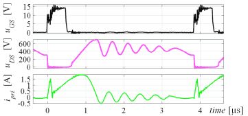
Fig. 2. Measured waveforms of resonant-mode operation, D = 0.6. (a) Switch Si voltage and current; (b) Current of each transformer winding (c) Snubber diode current, resonant capacitor voltage and current.

Fig.3. Measured waveforms of resonant flyback at high input voltage, Ui=360V, fs=250kHz, Po=38W.

CONCLUSION
In this paper, a flyback converter in resonant mode is proposed to enable soft switching, less transformer loss and reduced EMI at high switching frequency. Experimental results show that, compared to the conventional flyback converter operating in QR/DCM and while achieving the same specifications, both the fundamental quasi-peak and the high-frequency harmonics in the measured common-mode EMI are reduced due to the resonant behavior, and the switching loss on the primary switch is minimized due to the achieved soft switching in both turn-on and turn-off of the primary switch. Furthermore, the transformer core volume is reduced by one third compared to the low-frequency conventional flyback converter. In conclusion, the resonant-mode operation of the developed flyback converter enables higher power density, high efficiency and better EMI performance at high switching frequency. Therefore, the improved flyback topology is suitable for low-power isolated DC/DC converters with limited input voltage range.


REFERENCES
[1]   R. Watson; F.C. Lee; G.C. Hua, "Utilization of an active-clamp circuit to achieve soft switching in flyback converters," IEEE Transactions on Power Electronics, pp. 162 - 169, Jan 1996.
[2]   Y. Xi; P.K. Jain; G. Joos; Y. Liu, "An improved zero voltage switching flyback converter topology," in 29th Annual IEEE Power Electronics Specialists Conference, Fukuoka, May 1998.
[3]   Ching-Lung Chu; Ming-Juh Jong, "A zero-voltage-switching PWM flyback converter with an auxiliary resonant circuit," in International Conference on Power Electronics and Drive Systems, Taipei, Nov. 2009.
[4]   Y. Wei, X. Huang, J. Zhang and Z. Qian, "A Novel soft switching flyback converter with synchronous rectification," in IEEE 6th International Power Electronics and Motion Control Conference, Wuhan, May 2009.
[5]   "NCP4304: Secondary Side Controller," ON Semiconductor, 2015. [Online]. Available: http://www.onsemi.com/.


A PLL-Based Controller for Three-Phase Grid-Connected Power Converters

ABSTRACT
The current control of three-phase grid-connected converters is typically carried out by using a proportional resonant controller or synchronous reference frame proportional integral regulator. The implementation of these controllers often requires knowledge of the grid voltage frequency/phase angle, which is typically provided by a synchronization unit. It implies that dynamics and possible inaccuracies of the synchronization unit have a considerable impact on the current controller performance. The aim of this letter is to design an adaptive current controller by using a conventional synchronous reference frame phase-locked loop (SRF-PLL). In this way, the current controller and synchronization part are merged into a single unit, which results in a simpler and more compact structure. The effectiveness of the proposed controller is verified using experimental results.

KEYWORDS:
1.      Current control
2.      Distributed generation (DG) systems
3.      Phase-locked loop (PLL)
4.      Power converters
5.      Synchronization.

SOFTWARE: MATLAB/SIMULINK

CONTROL SYSTEM CIRCUIT DIAGRAM:

Fig. 1. Power stage of a three-phase VSC with the proposed PLL-based controller and a harmonic/imbalance compensator.

EXPECTED EXPERIMENTAL RESULTS:

Fig. 2. Experimental results for the test 1.

Fig. 3. Experimental results for the test 2.

Fig. 4. Experimental results for the test 3.

CONCLUSION
In this letter, a PLL-based controller for grid-connected converters was proposed. This controller, which is realized by adding a positive feedback loop to the conventional SRFPLL, eliminates the need for a dedicated synchronization unit and, therefore, results in a more compact structure. To enhance the harmonic/imbalance rejection capability of the suggested controller, multiple complex integrators tuned at low-order disturbance frequencies is employed. To simplify the tuning procedure, a simple yet accurate linear model describing the frequency estimation dynamics of the proposed controller was was verified using some experimental results. The main contribution of this letter is not the proposed controller. It is actually demonstrating the possibility of making a frequency-adaptive controller from a standard PLL. The importance of this contribution will be more evident when we notice that there are a large number of advanced PLLs which can be explored for the controller design.
REFERENCES
[1]   J. M. Carrasco, L. G. Franquelo, J. T. Bialasiewicz, E. Galvan, R. C. P. Guisado, M. A. M. Prats, J. I. Leon, and N. Moreno-Alfonso, “Powerelectronic systems for the grid integration of renewable energy sources: A survey,” IEEE Trans. Ind. Electron., vol. 53, no. 4, pp. 1002–1016, Jun. 2006.
[2]   F. Blaabjerg, Z. Chen, and S. B. Kjaer, “Power electronics as efficient interface in dispersed power generation systems,” IEEE Trans. Power Electron., vol. 19, no. 5, pp. 1184–1194, Sep. 2004.
[3]   B. K. Bose, “Power electronics and motor drives recent-progress and perspective,” IEEE Trans. Ind. Electron., vol. 56, no. 2, pp. 581–588, Feb. 2009.
[4]   F. Blaabjerg, R. Teodorescu, M. Liserre, and A. V. Timbus, “Overview of control and grid synchronization for distributed power generation systems,” IEEE Trans. Ind. Electron., vol. 53, no. 5, pp. 1398–1409, Oct. 2006.

[5]    Q. Zeng and L. Chang, “An advanced SVPWM-based predictive current controller for three-phase inverters in distributed generation systems,” IEEE Trans. Ind. Electron., vol. 55, no. 3, pp. 1235–1246, Mar. 2008.