asokatechnologies@gmail.com 09347143789/09949240245

Search This Blog

Sunday, 2 July 2017

Xilinx FPGA based multilevel PWM single phase inverter


ABSTRACT
In this paper a XILINX FPGA based multilevel PWM single-phase inverter was constructed by adding a bi-directional switchs to the conventional bridge topology. The inverter can produce three and five different output voltage levels across the load. XILINX FPGA is a programmable logic device developed by XILINX which is considered as an efficient hardware for rapid prototyping. It is used as a PWM generator to apply the appropriate signals to inverter switches. In addition to XILINX FPGA, Matlab/Simulink software was used for simulation and verification of the proposed circuit before implementation, Simulation and experimental results show that both are in close agreement.

SOFTWARE: MATLAB/SIMULINK

CIRCUIT DIAGRAM:

Fig.1 The proposed circuit of the multilevel PWM single phase inverter


EXPECTED SIMULATION AND EXPERIMENTALRESULTS:

Fig.2.Multilevel PWM single phase simulation results using XILINX FPGA at Ma = 0.8.

Fig.3 Multilevel PWM single phase simulation results using XILINX FPGA at Ma = 0.4.


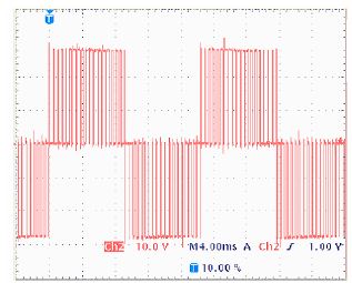
Fig.4 Multilevel single-phase PWM at Ma=0.8 Simulated, (b) Experimental


Fig.5 Multilevel single-phase PWM at Ma=0.4 (a) Simulated, (b) Experimental


     Fig.6.Unfiltered output voltage five levels at Ma=0.8

         
         Fig.7 Unfiltered output voltage five levels at Ma=0.4


Fig.8. Ac voltage waveform before and after the filter in the proposed multilevel PWM inverter at modulationindexes (a) 0.8 and (b) 0.4.


       Fig.9.Ac voltage and current output waveforms for
                resistive load.                                                                               


 Fig.10 Ac voltage and current output waveforms for (resistive- inductive) load.


Fig.11Ac voltage output harmonic spectral after filter


CONCLUSION

The switching patterns adopted are applied at the six inverter switches to generate five or three output voltage levels at different modulation indexes. XILINX FPGA enables to make easy, fast and flexible design and implementation. The experimental and simulated results are show satisfactory results in term of total harmonic distortion and output voltage and current waveform shapes.

REFERENCES
.
[1]   V.G.Agelidis, D.M.Baker, W.B.Lawrance and C.V. Nayar “ AMultilevel PWM Inverter Topology for Photovoltaic Applications” IEEE.ISIE’97,Guimaräes, Portugal, pp.589-594, 1997.
[2]    J.S. Lai and F.Z.Peng, ”Multilevel converters –A new breed of power conversion ” IEEE Trans. 1nd. Applicat., vol.32, pp. 509-517, May/June. 1996.
[3]   N.S. Choi, J.H. Cho, and G.H. Cho, “A General circuit Topology of Multilevel Inverter” IEEE Trans. Power Electronics, vol. 6, pp.96-103, 1991.
[4]   E. Cengelci, S. U. Sulistijo, B. O. Woom, P. Enjeti, R. Teodorescu, and F. Blaabjerge,“A new medium voltage PWM inverter topology for adjustable speed drives” in Conf. Rec. IEEE-IAS Annu. Meeting, St. Louis MO, pp.1416-1423, Oct.1998.
[5]    B. N. Mwinyiwiwa, Z.Wolanski, and B. T. Ooi, “Microp- rocessor implemented SPWM for multiconverters with phase-shifted triangle carriers” in Conf. Rec IEEE-IAS Annu. Meet- ing, NewOrleans, pp. 1542–1549, Oct. 1997.


Multilevel Inverter for Grid-Connected PV System Employing Digital PI Controller

ABSTRACT
This paper presents a single-phase five-level photovoltaic (PV) inverter topology for grid-connected PV systems with a novel pulse width-modulated (PWM) control scheme. Two reference signals identical to each other with an offset equivalent to the amplitude of the triangular carrier signal were used to generate PWM signals for the switches. A digital proportional–integral current control algorithm is implemented in DSP TMS320F2812 to keep the current injected into the grid sinusoidal and to have high dynamic performance with rapidly changing atmospheric conditions. The inverter offers much less total harmonic distortion and can operate at near-unity power factor. The proposed system is verified through simulation and is implemented in a prototype, and the experimental results are compared with that with the conventional single-phase three-level grid-connected PWM inverter.

KEYWORDS:
1.      DSP TMS320F2812
2.      Grid connected
3.      Photovoltaic (PV)
4.      Proportional–integral (PI) current control
5.      Pulse width modulated (PWM) inverter.

SOFTWARE: MATLAB/SIMULINK


CIRCUIT DIAGRAM:

Fig. 1. Single-phase five-level inverter topology.

EXPECTED SIMULATION RESULTS:

Fig. 2. Inverter output voltage (Vinv) and grid current (Ig) for different values of M. (a) Vinv forM <0.5. (b) Ig forM <0.5. (c) Vinv forM >1.0.(d) Ig forM >1.0. (e) Vinv for 0.5 M 1.0. (f) Ig for 0.5 M 1.0.

Fig. 3. Step response of the PI current control scheme.

CONCLUSION
This paper presented a single-phase multilevel inverter for PV application. It utilizes two reference signals and a carrier signal to generate PWM switching signals. The circuit topology, modulation law, and operational principle of the proposed inverter were analyzed in detail. A digital PI current control algorithm is implemented in DSP TMS320F2812 to optimize the performance of the inverter. Experimental results indicate that the THD of the five-level inverter is much lesser than that of the conventional three-level inverter. Furthermore, both the grid voltage and the grid current are in phase at near-unity power factor.

REFERENCES
[1]   J. M. Carrasco, L. G. Franquelo, J. T. Bialasiewicz, E. Galvan, R. C. PortilloGuisado, M. A. M. Prats, J. I. Leon, and N.Moreno-Alfonso, “Power-electronic systems for the grid integration of renewable energy sources: A survey,” IEEE Trans. Ind. Electron., vol. 53, no. 4, pp. 1002– 1016, Aug. 2006.
[2]   V. G. Agelidis, D. M. Baker, W. B. Lawrance, and C. V. Nayar, “A multilevel PWMinverter topology for photovoltaic applications,” in Proc. IEEE ISIE, GuimarĂ£es, Portugal, 1997, pp. 589–594.
[3]    S. Kouro, J. Rebolledo, and J. Rodriguez, “Reduced switching-frequencymodulation algorithm for high-power multilevel inverters,” IEEE Trans. Ind. Electron., vol. 54, no. 5, pp. 2894–2901, Oct. 2007.
[4]   S. J. Park, F. S. Kang, M. H. Lee, and C. U. Kim, “A new single-phase fivelevel PWM inverter employing a deadbeat control scheme,” IEEE Trans. Power Electron., vol. 18, no. 18, pp. 831–843, May 2003.

[5]    L. M. Tolbert and T. G. Habetler, “Novel multilevel inverter carrier-based PWM method,” IEEE Trans. Ind. Appl., vol. 35, no. 5, pp. 1098–1107, Sep./Oct.1999.

Saturday, 1 July 2017

FPGA-Based Pulse-Width Modulation Control for Single-Phase Multilevel Inverter

ABSTRACT
Presented is pulse-width modulation (PWM) for single-phase five-level inverter via field-programmable gate array (FPGA). The proposed inverter has conventional full bridge configuration and one bidirectional switch. The control technique is digitally generated based on multicarrier PWM in Altera DE2 board, which has many features that allow implementation of the system design through Cyclone II FPGA device. A sinusoidal reference signal and two triangular carrier signals in phase and of the same frequency but different offset voltages were used to generate the PWM signals for the inverter switches. Besides Altera Quartus II software, Matlab/Simulink software was used to simulate and verify the proposed circuit before it was implemented in a prototype hardware. Simulation and experiment results closely agreed.

KEYWORDS:
1.      Pulse-width modulation (PWM)
2.      FPGA
3.      Multilevel inverter.

SOFTWARE: MATLAB/SIMULINK

CIRCUIT DIAGRAM:

Figure 1. The five-level inverter equipped with LC filter and a resistive
load.
EXPECTED SIMULATION RESULTS:

Figure 2. Simulation results for PWM switching patterns on (a)Quartus II, (b) Matlab/Simulink.

Figure 3. Simulation result for the dead-time designed on Quartus II.

Figure 4. Simulation result for the output voltage waveforms, before and after filtering.

Figure 5, Simulation result for the output voltage and load current waveforms.


Figure 6. THD of the filtered ac voltage.

CONCLUSION
PWM switching patterns were applied to the proposed inverter switches to produce a five-level output voltage. Altera FPGA enabled fast, flexible design and implementation. Simulation and experiment results were satisfactory for pulse generation, the five-level output voltage and the filtered output voltage and current.

REFERENCES
[1]   S. Kouro, J. Rebolledo and 1. Rodriguez, "Reduced switching-frequency modulation algorithm for high-power multilevel inverters," IEEE Trans. Ind. Electron., vol. 54, no. 5, pp. 2894-2901, Oct. 2007.
[2]    1. Rodriguez, J. S. Lai and F. Z. Peng, "Multilevel inverters: A survey of topologies, controls, and applications," IEEE Trans. Ind. Electron., vol. 49, no. 4, pp.724-738, Aug. 2002.
[3]    1. Rodriguez, L.G. Franquelo, S. Kouro, J.1. Leon, R.C. Portillo, M.A.M. Prats and M.A. Perez, "Multilevel converters : An enabling technology for high-power applications," Proc of the [EEE, vol. 97, no. [I, pp. 1786-1817 , Nov. 2009.
[4]   D. Puyal, L.A. Barragan, 1. Acero, 1. M. Burdio and I. Millan, "An FPGA-based digital modulator for full- or half-bridge inverter control" IEEE Trans. Power Electron., vol. 21, no. 5, pp. 1479-1483, Sept. 2006.

[5]   S. Mekhilef and A. Masaoud, "Xilinx FPGA based multilevel PWM single phase inverter," 2006 Engineering e-Transaction, vol.l, no.2, pp 40-45, Dec. 2006.

FPGA based Cascaded Multilevel Pulse Width Modulation for Single Phase Inverter

ABSTRACT
This article explores the development of FPGA based controller for conventional and cascaded multilevel PWM single phase inverter. The conventional multilevel inverter is constructed by the H-bridge and cascaded multilevel inverter constructed by two full H-bridges. FPGA logic device is chosen for the hardware implementation of control circuit. VHDL language is used to model the inverter switching strategies. The proposed controller generates 4 and 8 control signals for conventional multilevel inverter and cascaded multilevel inverter respectively. These inverters provide 3-level and 7- level output voltages. Matlab/System generator and XILINX are used as a simulation and compiler architecture of control circuit embedded in FPGA. These inverter topologies with filters would have reduced harmonics and can operate at high efficiency.

KEYWORDS:
1.      Field Programmable gate array (FPGA)
2.      VHDL Hardware description language
3.      Multilevel inverter
4.       Cascaded multilevel inverter
5.      Digital controller.


SOFTWARE: MATLAB/SIMULINK

CIRCUIT DIAGRAMS:


Fig 1.Conventional multilevel PWM single phase inverter


Fig 2. Cascade PWM single phase inverter with a single DC supply source.

EXPECTED SIMULATION RESULTS:

Fig 3. three -level multilevel PWM single phase inverter output voltage


Fig 4.three-level multilevel PWM single phase inverter output current


Fig 5. order of harmonic measured with respect to the magnitude of the
fundamental frequency for single phase conventional multilevel VSI


Fig 6.seven -level cascaded PWM single phase inverter output voltage


Fig 7. seven-level cascaded PWM single phase inverter output current


Fig 8.order of harmonic measured with respect to the magnitude of the
fundamental frequency for single phase Cascaded multilevel VSI

CONCLUSION
The FPGA based controller switching patterns are adopted and applied to the multilevel inverter and cascaded multilevel inverter switches to generate 3-level and 7-level output voltages respectively. The FPGA enables to make easy, fast and flexible design of the control circuit for hardware implementation. It can effectively extend the modulation index range that facilitates a better quality output voltage with minimal distortion. The experimental and simulation results demonstrate quality voltage and current waveform shapes at the output of the inverter. These inverter topologies with proposed control circuit can be used for speed control of induction motor and other industrial applications and would be attempted as a future work.

REFERENCES
[1]   .Keith Corzine and Yakov Familiant “A New Cascaded Multilevel HBridge Drive”- IEEE Trans on power electronics, Vol.17, no.1, Jan-2002
[2]    John N. Chiasson, Burak Ă–zpineci, and Leon M. Tolbert “A Five-Level Three-Phase Hybrid Cascade Multilevel Inverter Using a Single DC Source for a PM Synchronous Motor Drive- 2007 IEEE.
[3]   Zhong Du, Burak Ozpineci, and Leon M. Tolbert “Modulation Extension Control of Hybrid Cascaded H-bridge Multilevel Converters with 7-level Fundamental Frequency Switching Scheme” Oak Ridge National Laboratory, Oak Ridge
[4]    M.I. Ahmad, Z. Husin, R. B. Ahmad, H. A Rahim, M.S. Abu Hassan, M.N. Md Isa “FPGA based control IC for Multilevel Inverter” Proceedings of the International Conference on Computer and Communication Engineering 2008

[5]   S. Mekhilef and Masaoud “Xilinx FPGA Based Multilevel PWM Single Phase Inverter” Engineering e-Transaction, Vol.1, No 2, pp 40-45, 2006

Thursday, 29 June 2017

A Primary Full-Integrated Active Filter Auxiliary Power Module in Electrified Vehicles with Single-Phase On board Chargers

ABSTRACT


 In single-phase ac high-voltage (HV) battery chargers, as the input current is enforced to be varying sinusoidally in phase with the input voltage, the pulsating power at two times of the line frequency will be seen on the dc-link. Bulky capacitor bank or extra active filter circuits are needed to assimilate this harmonic current, which become a major barrier in terms of power density and cost. Sinusoidal charging method can be applied, while this might affect the charging efficiency and a deep study is still needed to further investigate on the impact to the Lithium-ion battery. An active filter auxiliary power module (AFAPM) based dual-mode dual-voltage charging system for vehicle application has been proposed. The AFAPM converter has two modes: 1) the HV active filtering mode, in which the vehicle is connected to the grid and the converter assimilates the significant second-order harmonic current; 2) the low-voltage (LV) battery charging mode, in which the vehicle is running and the converter charges the LV battery from HV battery. However, a relay and inductors are still required in that converter to achieve the dual-mode operation. This paper proposes a primary full-integrated AFAPM for electrified vehicle applications with single-phase onboard chargers. The proposed AFAPM converter is composed of a two-phase bidirectional buck converter to work as an active filter (AF) and a dual-active-bridge (DAB) to operate as a LV battery charger auxiliary power module (APM). With the proposed converter, only an extra active energy storage capacitor is needed to achieve the active filtering. All the switches and inductors on the primary stage are shared between the AF and APM. Therefore, the use of a bulky capacitor bank or an additional AF circuit is avoided and thus, the cost, size and weight of the dual-voltage charging system in the electrified vehicle applications can be reduced. To confirm the effectiveness of the proposed converter, a 720 W prototype.

KEYWORDS:
1.      Active filters, auxiliary power modules
2.      Dc/Dc converters
3.      Dual-voltage charging systems
4.      Plug-in hybrid electric vehicles
5.      Single-phase chargers.

SOFTWARE: MATLAB/SIMULINK

CIRCUIT DIAGRAM:
Fig. 1: The dual-voltage charging system with the proposed primary full-integrated AFAPM.

EXPECTED SIMULATION RESULTS:

Fig. 2: Simulation results of AF mode, (a) HV dc-link voltage vdc, (b) capacitor Cr voltage vcr, (c) transformer primary voltage vpri, (d) inductor Lra and Lrb current ira and irb, (e) capacitor Cr current icr.

Fig. 3: Simulation results of APM mode, (a) transformer primary voltage vpri, (b) transformer secondary voltage vsec, (c) inductor Lra and Lrb current ira and irb, (d) LV output current iLo, (e) capacitor Cr voltage vcr

CONCLUSION
In this paper, a new primary full-integrated AFAPM converter is proposed. The proposed converter is not only a LV battery charger APM, but also an AF for the HV battery charger. A full bridge and auxiliary inductors are shared between the DAB APM converter and the two phase buck AF converter. Only an active harmonic energy storage capacitor is needed to achieve active filtering. As a result, from the harmonic energy storage aspect for the 6.6 kW HV battery charger in the vehicle applications, with the proposed AFAPM method, the volume and cost can decrease to 45.8% and 44.7% of the volume and cost of the conventional extra active filter method, respectively.  A 720 W prototype has been built and experiments show promising results confirming the effectiveness of the proposed converter.

REFERENCES
.
[1]   L. Xue, Z. Shen, D. Boroyevich, P. Matavelli, and D. Diaz, “Dual active bridge-based battery charger for plug-in hybrid electric vehicle with charging current containing low frequency ripple,” IEEE Transactions on Power Electronics, vol. 30, no. 12, pp. 7299-7307, Dec. 2015.
[2]   B. Bilgin, P. Magne, P. Malysz, Y. Yang, V. Pantelic, M. Preindl, A. Korobkine, W. Jiang, M. Lawford, and A. Emadi, “Making the case for electrified transportation,” IEEE Transactions on Transportation Electrification, vol. 1, no. 1, pp. 4-17, Jun. 2015.
[3]   S. Jahdi, O. Alatise, C. Fisher, R. Li, and P. Mawby, “An evaluation of silicon carbide unipolar technologies for electric vehicle drive-trains,” IEEE Journal of Emerging and Selected Topics in Power Electronics, vol. 2, no. 3, pp. 517–528, Sep. 2014.
[4]    H. A. Mantooth, M. D. Glover, and P. Shepherd, “Wide bandgap technologies and their implications on miniaturizing power electronic systems,” IEEE Journal of Emerging and Selected Topics in Power Electronics, vol. 2, no. 3, pp. 374-385, Sep. 2014.