asokatechnologies@gmail.com 09347143789/09949240245

Search This Blog

Wednesday, 25 April 2018

High-Frequency AC-Link PV Inver


ABSTRACT:
In this paper, a high-frequency ac-link photovoltaic (PV) inverter is proposed. The proposed inverter overcomes most of the problems associated with currently available PV inverters. In this inverter, a single-stage power-conversion unit fulfills all the system requirements, i.e., inverting dc voltage to proper ac, stepping up or down the input voltage, maximum power point tracking, generating low-harmonic ac at the output, and input/output isolation. This inverter is, in fact, a partial resonant ac-link converter in which the link is formed by a parallel inductor/capacitor (LC) pair having alternating current and voltage. Among the significant merits of the proposed inverter are the zero-voltage turn-on and soft turn-off of the switches which result in negligible switching losses and minimum voltage stress on the switches. Hence, the frequency of the link can be as high as permitted by the switches and the processor. The high frequency of operation makes the proposed inverter very compact. The other significant advantage of the proposed inverter is that no bulky electrolytic capacitor exists at the link. Electrolytic capacitors are cited as the most unreliable component in PV inverters, and they are responsible for most of the inverters’ failures, particularly at high temperature. Therefore, substituting dc electrolytic capacitors with ac LC pairs will significantly increase the reliability of PV inverters. A 30-kW prototype was fabricated and tested. The principle of operation and detailed design procedure of the proposed inverter along with the simulation and experimental results are included in this paper. To evaluate the long-term performance of the proposed inverter, three of these inverters were installed at three different commercial facilities in Texas, USA, to support the PV systems. These inverters have been working for several months now.
KEYWORDS:
1.      Inverters
2.      Photovoltaic (PV) systems
3.      Zero voltage switching
SOFTWARE: MATLAB/SIMULINK

CIRCUIT DIAGRAM:


Fig. 1. Proposed PV inverter.

EXPECTED SIMULATION RESULTS:


Fig. 2. PV current and voltage at full power.


Fig. 3. AC-side current and voltage at full power.


Fig. 4. Link voltage at full power.


Fig. 5. Link current at full power.


         Fig. 6. Link current and voltage at full power, using 0.1-μF link capacitance.

Fig. 7. Link current and voltage at 15 kW.

Fig. 8. AC-side current and voltage when the irradiance drops from 850 to
650 w/m2.

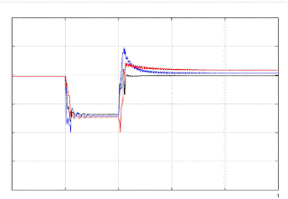
Fig. 9. AC-side current and voltage when the temperature changes from
25 C to 50 C.

Fig. 10. AC-side current and voltage when the AC-side voltage drops to 10%
of its nominal value (at t = 0.016 s).

Fig. 11. PV current and voltage when the AC-side voltage drops to 10% of its
nominal value (at t = 0.016 s).

CONCLUSION:
In this paper, a reliable and compact PV inverter has been proposed. This inverter is a partial resonant ac-link converter in which the link is formed by an LC pair having alternating current and voltage. The proposed converter guarantees the isolation of the input and output. However, if galvanic isolation is required, the link inductance can be replaced by a singlephase high-frequency transformer. The elimination of the dc link and low-frequency transformer makes the proposed inverter more compact and reliable compared with other types of PV inverters. In this paper, the principle of operation of the proposed converter along with the detailed design procedure has been presented. The performance of the proposed converter has been evaluated through both simulation and experimental results.
 REFERENCES:
[1] S. Chakraborty, B. Kramer, and B. Kroposki, “A review of power electronics interfaces for distributed energy systems towards achieving low-cost modular design,” Renew. Sustain. Energy Rev., vol. 13, no. 9, pp. 2323–2335, Dec. 2009.
[2] Y. Huang, F. Z. Peng, J. Wang, and D. W. Yoo, “Survey of the power conditioning system for PV power generation,” in Proc. IEEE PESC, Jun. 18–22, 2006, pp. 1–6.
[3] S. Atcitty, J. E. Granata, M. A. Quinta, and C. A. Tasca, Utility-scale gridtied PV inverter reliability workshop summary report, Sandia National Labs., Albuquerque, NM, USA, SANDIA Rep. SAND2011-4778. [Online].
Available: http://energy.sandia.gov/wp/wp-content/gallery/uploads/  Inverter_Workshop_FINAL_072811.pdf
[4] Y. C. Qin, N. Mohan, R. West, and R. Bonn, Status and needs of power electronics for photovoltaic inverters, Sandia National Labs., Albuquerque, NM, USA, SANDIA Rep. SAND2002-1535. [Online]. Available: www.prod.sandia.gov/techlib/access-control.cgi/2002/021535. pdf
[5] T. Kerekes, R. Teodorescu, P. Rodríguez, G. Vázquez, and E. Aldabas, “A new high-efficiency single-phase transformerless PV inverter topology,” IEEE Trans. Ind. Electron., vol. 58, no. 1, pp. 184–191, Jan. 2011.

Tuesday, 17 April 2018

Comparative Simulation Results of DVR and D-STATCOM to Improve Voltage Quality in Distributed Power System


ABSTRACT:
This paper presents the comparative improvement of the voltage profile of the distributed power system using a Dynamic Voltage Restorer (DVR) and a Distributed Static Synchronous Compensator (D-STATCOM). The IEEE benchmark 13-bus distributed power system is used to present the distributed power grid. A proposed DVR is connected in series with bus 632 while a D-STATCOM is connected in parallel with bus 632. Comparative simulation results of the system with DVR and D-STATCOM are performed by using commercial MATLAB software. It can be concluded from the simulation results that DVR is suitable to mitigate the voltage sag of the load side while D-STATCOM can enhance the voltage stability margin of the buses that are located near the connected bus of the proposed D-STATCOM in the distributed grid.

KEYWORDS:
1.      Distributed Power System
2.      Dynamic Voltage Restorer (DVR)
3.      Distributed Static Synchronous Compensator (D-STATCOM)
4.      Voltage Quality.

SOFTWARE: MATLAB/SIMULINK

DVR AND STATCOM MODELS:
Figure 1. Basic DVR Model

Figure 2. Basic D-STATCOM Model

EXPECTED SIMULATION RESULTS:
a.       Voltage at bus 633 without DVRlD-STATCOM
b.      Voltage at bus 646 with D-STATCOM
c.       Voltage at bus 633 with D-STATCOM
d.      Voltage at bus 684 with D-STATCOM
e.       Voltage at bus 646 with DVR

f.       Voltage at bus 633 with DVR
g.      Voltage at bus 684 with DVR
Figure 3. Simulation results of the studied system when a three-phase short-circuit fault happened at bus 633.

CONCLUSION:
In this paper, the voltage stability improvement of an IEEE I3-bus distributed power system has been presented. A DVR and a D-STATCOM have been proposed and integrated to the studied system. Based on the results from the simulation, it can be concluded that the proposed DSTATCOM is better than DVR for improving the voltage quality of the distributed power system under a severe fault happened.


REFERENCES:
[1]   M. Bollen, "Understanding Power Quality Problems - Voltage Sags and Interruptions", IEEE Press Series on Power Engineering – John Wiley and Sons, Piscataway, USA, 2000.
[2]   Math H.J. Bollen, Understanding power quality problems: voltage sags and interruptions, IEEE Press, New York, 2000.
[3]   FACTS controllers in power transmission and distribution by K. R. Padiyar ISBN: 978-81-224-2541-3.
[4]   B. Singh, A. Adya, A. P. Mittal and J. R. P. Gupta, "Modeling, Design and Analysis of Different Controllers for DSTATCOM," 2008 Joint International Conference on Power System Technology and IEEE Power india Conference, New Delhi, 2008, pp. 1-8.
[5]   Devaraju, V. C. Reddy and M. Vijaya Kumar, "Performance of DVR under different voltage sag and swell conditions", ARPN Journal of Engineering and Applied Sciences, Vol. 5, No. 10,2010, pp. 56-64.

Nine-level Asymmetrical Single Phase Multilevel Inverter Topology with Low switching frequency and Reduce device counts


ABSTRACT:
This paper presents a new asymmetrical single phase multilevel inverter topology capable of producing nine level output voltage with reduce device counts. In order to obtain the desired output voltage, dc sources are connected in all the combination of addition and subtraction through different switches. Proposed topology results in reduction of dc source, switch counts, losses, cost and size of the inverter. Comparison between the existing topologies shows that the proposed topology yields less component counts. Proposed topology is modeled and simulated using Matlab-Simulink software in order to verify the performance and feasibility of the circuit. A low frequency switching strategy is also proposed in this work. The results show that the proposed topology is capable to produce a nine-level output voltage with less number of component counts and acceptable harmonic distortion content.
KEYWORDS:
1.      Multilevel inverter
2.      Asymmetrical
3.      Total Harmonic Distortion (THD)
4.      Low-frequency switching

SOFTWARE: MATLAB/SIMULINK

 CIRCUIT DIAGRAM:

Fig. 1. Proposed nine level inverter topology.

EXPECTED SIMULATION RESULTS:


(a)     Output voltage waveform

(b)     Voltage Output Harmonic spectrum

(c)     Load current waveform

(d)     Load Current Harmonic spectrum

Fig. 2. Simulation Output results at 50Hz fundamental frequency for R = 150ohm, L= 240, P.F = 0.9


(a)     Output voltage waveform

(b)        Voltage Output Harmonic spectrum


(c)     Load current waveform

(d)     Load Current Harmonic spectrum
Fig. 3. Simulation Output results at 50Hz fundamental frequency for R = 150ohm, L= 240, P.F = 0.9
CONCLUSION:
In this paper a new single-phase multilevel inverter topology is presented. Proposed topology is capable of producing nine-level output voltage with reduce device counts. It can be used in medium and high power application with unequal dc sources. Different modes of operation are discussed in detail. On the bases of device counts, the proposed topology is compared with conventional as well as other asymmetrical nine-level inverter topologies presented in literature. Comparative study shows that, for nine level output, the proposed topology requires lesser component counts then the conventional and other topologies. Proposed circuit is modeled in Matlab/Simulink environment. Results obtained shows that topology works properly. Detailed Simulation analysis is carried out. THD obtained in the output voltage is 8.95% whereas the each harmonic order is < 5%, satisfies harmonic Standard (IEEE-519).
 REFERENCES:
[1] J. Rodriguez, L. G. Franquelo, S. Kouro, J. I. Leon, R. C. Portillo, M. A. M. Prats and M. A. Perez, “Multilevel Converters: An Enabling Technology for High-Power Applications”, IEEE Proceeding, Vol 97, No. 11, pp.1786 – 1817, November 2009.
[2] J. R. Espinoza, “Inverter”, Power Electronics Handbook, M. H. Rashid, Ed. New York, NY, USA: Elsevier, 2001,pp. 225 -269.
[3] L. M. Tolbert and T. G. Habetler, “Novel multilevel inverter carrier based PWM method”, IEEE Transactions on Indsutrial Apllications”, Vol. 35, No. 5, pp. 1098-1107, September 1999.
[4] S. Debnath, J. Qin, B. Bahrani, M. Saeedifard and P. Barbosa, “Operation, Control and Applications of the Modular Multilevel Converter: A Review”, IEEE Transactions on Power Electronics, Vol. 30, No. 1, pp. 37-53, January 2015.
[5] L. G. Franquelo, J. Rodriguez, J. I. Leon, S. Kouro, R. C. Portillo and M. A. M. Prats, “The Age of Multilevel Converters Arrives”, IEEE Industrial Electronics magazine, Vol. 2, No. 2 pp. 28-39, June 2008.

Performance of Electric Springs with Multiple Variable Loads


ABSTRACT:
Electric Spring is an emerging smart grid technology, which can provide voltage support to weakly regulated system. This paper studies the effect of load variation on the performance of electric springs. Two different single phase circuits with intermittent power supply have been simulated for the study – with one electric spring and with two electric springs. The loads considered are linear and are identical. Results obtained in MATLAB/Simulink environment show that line voltage is regulated by electric spring irrespective of variation in load. A brief comparative study is done between the simulation results obtained from the two circuits to observe the effect of the additional electric spring. This study tests the effectiveness of electric springs in a circuit designed to be more realistic, i.e., when the loads are not ON all the time and multiple electric springs are distributed all over the grid.

KEYWORDS:
1.      Demand Side Management
2.      Electric Spring
3.      Renewable Energy Sources

SOFTWARE: MATLAB/SIMULINK

 SCHEMATIC DIAGRAM:


Fig. 1. Schematic Diagram of Electric Spring connected with Intermittent Renewable Energy Source

BLOCK DIAGRAM:

Fig. 2. Block Diagram for Circuit with Two Electric Springs
EXPECTED SIMULATION RESULTS:


Fig. 3. RMS Voltage for Boosting action in single ES circuit

Fig. 4. Active and Reactive power consumption of ES during Boosting action in single ES circuit


Fig. 5. RMS Voltage for Reduction action in single ES circuit

Fig. 6. Active and Reactive power consumption of ES during Reduction action in single ES circuit

Fig. 7. RMS Voltage for Boosting action in double ES circuit

Fig. 8. Active and Reactive power consumption of ES during Boosting action in double ES circuit

Fig. 9. RMS Voltage for Reduction action in double ES circuit

Fig. 10. Active and Reactive power consumption of ES during Reduction action in double ES circuit


CONCLUSION:
This paper demonstrates the effects of load variation on the performance of ES. From the simulation results, it can be noted that, for boosting mode of operation, the ES can regulate the line voltage at the reference value irrespective of variation in load. However, for reduction mode of operation, the load variation causes fluctuations in the line voltage even when the ES is operating. This might be improved by making the circuit more inductive, which will assist the ES for reduction action. The basic single ES circuit was modified by adding an extra ES to it. It was observed that the reactive power consumption of each ES decreased by almost 50% for both modes of operation. Therefore we can conclude that as the number of ES in the circuit increases by a factor of ‘n’, the reactive power consumed by each ES to carry out the same magnitude of regulation decreases by a factor of ‘n’. This decreases the stress on each ES as well as the inverter rating for ES. For this study, the linear and identical loads have been considered, which can be further extended to non-linear and non-identical loads. Also, the random load profile can be replaced with a real time load profile.
REFERENCES:
[1] IEA, World Energy Outlook 2015: IEA. Available:
[2] P. P. Varaiya, F. F. Wu and J. W. Bialek, "Smart Operation of Smart Grid: Risk-Limiting Dispatch," in Proceedings of the IEEE, vol. 99, no. 1, pp. 40-57, Jan. 2011.
[3] D. Westermann and A. John, "Demand Matching Wind Power Generation With Wide-Area Measurement and Demand-Side Management," in IEEE Transactions on Energy Conversion, vol. 22, no. 1, pp. 145-149, March 2007.
[4] P. Palensky and D. Dietrich, "Demand Side Management: Demand Response, Intelligent Energy Systems, and Smart Loads," in IEEE Transactions on Industrial Informatics, vol. 7, no. 3, pp. 381-388, Aug. 2011.
[5] A. Mohsenian-Rad, V. W. S. Wong, J. Jatskevich, R. Schober, and A. Leon-Garcia, “Autonomous demand-side management based on gametheoretic energy consumption scheduling for the future smart grid,” IEEE Trans. Smart Grid, vol. 1, no. 3, pp. 320–331, Dec. 2010.