ABSTRACT:
This paper presents analysis and design of zero voltage
switching (ZVS) active-clamped current-fed full-bridge isolated dc/dc converter
for fuel cell applications. The designed converter maintains ZVS of all
switches from full load down to very light load condition over wide input
voltage variation. Detailed operation, analysis, design, simulation, and
experimental results for the proposed design are presented. The additional auxiliary
active clamping circuit absorbs the turn-off voltage spike limiting the peak
voltage across the devices allowing the selection and use of low-voltage
devices with low on-state resistance. In addition, it also assists in achieving
ZVS of semiconductor devices. The converter utilizes the energy stored in the
transformer leakage inductance aided by its magnetizing inductance to maintain
ZVS. ZVS range depends upon the design, in particular the ratio of leakage and
magnetizing inductances of the transformer. Rectifier diodes operate with
zero-current switching. An experimental converter prototype rated at 500 W has
been designed, built, and tested in the laboratory to verify the analysis,
design, and performance for wide variations in input voltage and load.
KEYWORDS:
1.
Fuel cells
2.
High-frequency
(HF) dc/dc converter
3.
Renewable
energy systems
4.
Zero voltage switching
(ZVS)
SOFTWARE: MATLAB/SIMULINK
CIRCUIT DIAGRAM:
Fig.
1. Active-clamped ZVS current-fed full-bridge dc-dc converter.
EXPECTED SIMULATION RESULTS:
Fig.
2. Simulation waveforms at Vin = 22 V and full load: (a)
voltage vAB, leakage inductance current ilk,
and magnetizing inductance current iLm (b) main switches’
currents iS1 and iS2,
auxiliary switch’s current iSax and voltage across auxiliary
capacitor VCa.
Fig.
3. Simulation waveforms at Vin = 41 V and 10% load: (a) voltage
vAB, leakage inductance current ilk, and
magnetizing inductance current iLm (b) main switches’
currents iS1 and iS2,
auxiliary switch’s current iSax and voltage across auxiliary
capacitor VCa.
Fig.
4. Experimental waveforms at Vin = 22 V and full load: (a)
Voltage vAB (100 V/div) and leakage inductance current ilk
(50 A/div), (b) main switch voltage vDS (50 V/div) and
gate voltage vGS (10 V/div), (c) auxiliary switch voltage vDS
(50 V/div) and gate voltage vGS (20 V/div), (d) main
switch current iS1 (20 A/div), (e) auxiliary
switch current iSax (20 A/div) and (f) magnetizing inductance
current iLm (0.5 A/div).
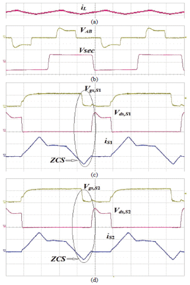
Fig.
5. Experimental waveforms at Vin = 41 V and full load: (a)
Voltage vAB (50 V/div) and leakage inductance current ilk
(50 A/div), (b) main switch voltage vDS (50 V/div) and
gate voltage vGS (10 V/div), (c) auxiliary switch voltage vDS
(50 V/div) and gate voltage vGS (20 V/div), (d) main
switch current iS1 (20 A/div), (e) auxiliary
switch current iSax (10 A/div) and (f) magnetizing inductance
current iLm (1 A/div).
Fig.
6. Experimental waveforms at Vin = 22 V and 20% load: (a)
Voltage vAB (50 V/div) and leakage inductance current ilk
(10 A/div), (b) main switch voltage vDS (50 V/div), gate
voltage vGS (20 V/div) and current iS1
(10 A/div), (c) auxiliary switch voltage vDS (50 V/div) and
gate voltage Vgs (10 V/div), (d) auxiliary switch current iSax
(5 A/div) and (e) magnetizing inductance current iLm (0.5
A/div).
Fig.
7. Experimental waveforms at Vin = 41 V and 10% load. (a)
Voltage vAB (50 V/div) and leakage inductance current ilk
(10 A/div), (b) main switch voltage vDS
(50 V/div) and gate voltage vGS (10 V/div), (c) auxiliary switch voltage vDS (50
V/div) and gate voltage vGS (10 V/div), (d) main switch
current iS1 (10 A/div), (e) auxiliary switch
current iSax (5 A/div) and (f) magnetizing inductance current
iLm (1 A/div).
CONCLUSION:
To
achieve ZVS for wide source voltage variation and varying output power/load
while maintaining high efficiency has been a challenge, particularly for
low-voltage higher current input applications. A ZVS active-clamped current-fed
full bridge isolated converter has been restudied in this paper. The
magnetizing inductance increases the leakage inductance current value at light
load and therefore the energy stored in leakage inductance to maintain ZVS of
main switches as well as auxiliary switch.
Detailed steady-state operation and analysis of
current-fed full-bridge converter have been presented. Design to attain soft switching
over an extended range of input voltage and load i.e., output power has been
presented. Simulation results using PSIM 9.0.4 have been presented. An experimental prototype of. the
converter rated at 500Whas been designed, built, and tested for variations in
input voltage and load in order to validate the analysis. Experimental results
verify the accuracy of the analysis and show that the proposed configuration is
able to maintain ZVS of all switches over a wide range of load and input
voltage variation due to the variation in fuel flow and stack temperature.
Theoretically, the converter is able to maintain ZVS till 20% load at 22 V and
5% load 41 V.
In a practical fuel cell application, when the load
current drops due to reduced fuel flow, the light or reduced power below rated
power is transferred at higher fuel cell voltage. It can be clearly seen and
understood also from the fuel cell V –I characteristic. If the
load current or power is around 10% of the rated power, then the fuel cell
stack voltage increases nearly to 41 V. Hence, the possibility of the condition
Vin = 22 V at 10% load is only during transition period when load is
suddenly changed from full load to 10% due to fuel flow adjustment. Hence, it
is justifiable to have ZVS range of 20% load at low input
voltage and below 10% at higher input voltage will cover the operating range at
steady state. Rated converter efficiency of 94% is obtained for the developed
lab prototype rated at 500 W. The converter has limitation that duty cycle of
the main switch should be greater than 50%.
REFERENCES:
[1]
S. Jain and V. Agarwal, “An integrated hybrid power supply for distributed generation
applications fed by nonconventional energy sources,” IEEE Trans. Energy
Convers., vol. 23, no. 2, pp. 622–631, Jun. 2008.
[2]
Y. Lembeye, V. D. Bang, G. Lefevre, and J. P. Ferrieux, “Novel half-bridge inductive
dc-dc isolated converters for fuel cell applications,” IEEE Trans. Energy
Convers., vol. 24, no. 1, pp. 203–210, Mar. 2009.
[3]
J. Mazumdar, I. Batarseh, N. Kutkut, and O. Demirci, “High frequency low cost
dc-ac inverter design with fuel cell source home applications,” in Conf.
Rec. IEEE IAS Annu. Meeting, Oct. 2002, vol. 2, pp. 789–794.
[4]
J. Wang, F. Z. Peng, J. Anderson, A. Joseph, and R. Buffenbarger, “Low cost
fuel cell converter system for residential power generation,” IEEE Trans.
Power Electron., vol. 19, no. 5, pp. 1315–1322, Sep. 2004.
[5]
R. Gopinath, S. Kim, J.-H. Hahn, P. N. Enjeti, M. B. Yeary, and J. W. Howze,
“Development of a low cost fuel cell inverter system with DSP control,” IEEE
Trans. Power Electron., vol. 19, no. 5, pp. 1256–1262, Sep. 2004.