ABSTRACT
Due
to the still increasing penetration of grid connected Photovoltaic (PV)
systems, advanced active power control functionalities have been introduced in
grid regulations. A power reserve control, where namely the active power from the
PV panels is reserved during operation, is required for grid support. In this
paper, a cost-effective solution to realize the power reserve for two-stage
grid-connected PV systems is proposed. The proposed solution routinely employs
a Maximum Power Point Tracking (MPPT) control to estimate the available PV
power and a Constant Power Generation (CPG) control to achieve the power
reserve. In this method, the solar irradiance and temperature measurements that
have been used in conventional power reserve control schemes to estimate the
available PV power are not required, and thereby being a sensorless approach with
reduced cost. Experimental tests have been performed on a 3-kW two-stage
single-phase grid-connected PV system, where the power reserve control is
achieved upon demands.
KEYWORDS:
1. Active
power control
2. Power
reserve control
3. Maximum
power point tracking
4. Constant
power generation control
5. PV
systems
6. Grid-connected
power converters.
SOFTWARE: MATLAB/SIMULINK
BLOCK
DIAGRAM:

Fig.1.System
configuration and control structure of a two-stage grid connected
PV system with the Sensorless Power
Reserve Control strategy.
EXPECTED EXPERIMENTAL RESULTS:


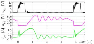
Fig.
2. Experimental results of the single-phase grid-connected PV system
with
the proposed SPRC strategy during the steady-state operation (solar
irradiance
level: 1000 W/m2; ambient temperature: 250C; available power
estimation
rate: fAPE = 0.2 Hz), where the reference power reserve ∆P are
700
W, 500 W, and 300 W: (a) PV voltage vpv, (b) PV power Ppv
and ac
power (Pac), (c) dc-link
voltage vdc, and (d) reserved power ∆P.

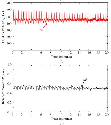
Fig.
3. Experimental results of the single-phase grid-connected PV system
with
the proposed SPRC strategy at the sampling rate of fAPE = 0.05 Hz
under
a ramp-changing solar irradiance profile (ambient temperature: 250C),
where
the reference power reserve ∆P is 500 W: (a) PV voltage vpv, (b)
PV
power Ppv and ac power (Pac), (c) dc-link voltage vdc,
and (d) reserved
power ∆P.


Fig.
4. Experimental results of the single-phase grid-connected PV system
with
the proposed SPRC strategy at the sampling rate of fAPE = 0.2 Hz
under
a
ramp-changing solar irradiance profile (ambient temperature: 250C),
where
the
reference power reserve ∆P is 500 W: (a) PV voltage vpv, (b) PV
power
Ppv and ac power (Pac),
(c) dc-link voltage vdc, and (d) reserved power ∆P.


Fig.
5. Zoomed-in view of the results in Fig. 16: (a) PV voltage vpv, (b)
PV
power
Ppv and ac power (Pac), (c) dc-link voltage vdc, (d)
reserved power P.

Fig.
6. Experimental result of the PV voltage vpv and the dc-link voltage
vdc with different
available power estimation sampling rates fAPE.
CONCLUSION
A
cost-effective sensorless power reserve control strategy for two-stage
grid-connected PV systems has been proposed in this paper. The
cost-effectiveness of the proposal lies in the sensorless estimation of the
available PV power, which is achieved by routinely employing a fast MPPT
operation. Then, the estimated available power is used for calculating the
set-point to limit the extracted PV power with the CPG operation. At the
grid-side, the stored energy in the dc-link is adaptively controlled to
minimize the power fluctuation during the available PV power estimation
process, where the excessed energy is temporarily stored in the dc-link. With the
above coordinated control strategy, the power reserve control can be achieved
as it has been verified experimentally. Design considerations for a high
control performance and the operational boundary have also been discussed to
assist the practical implementations.
REFERENCES
[1] REN21,
“Renewables 2016: Global Status Report (GRS),” 2016. [Online]. Available: http://www.ren21.net/.
[2] Fraunhofer ISE, “Recent Facts about
Photovoltaics in Germany,” April 22, 2016. [Online]. Available: http://www.pv-fakten.de/.
[3] Solar
Power Europe, “Global Market Outlook For Solar Power 2015 - 2019,” 2015.
[Online]. Available: http://www.solarpowereurope.org/.
[4] E.
Reiter, K. Ardani, R. Margolis, and R. Edge, “Industry perspectives on advanced
inverters for us solar photovoltaic systems: Grid benefits, deployment challenges,
and emerging solutions,” National Renewable Energy Laboratory (NREL), Tech.
Rep. No. NREL/TP-7A40-65063., 2015.
[5] Y.
Yang, P. Enjeti, F. Blaabjerg, and H. Wang, “Wide-scale adoption of
photovoltaic energy: Grid code modifications are explored in the distribution
grid,” IEEE Ind. Appl. Mag., vol. 21, no. 5, pp. 21–31, Sep. 2015..