asokatechnologies@gmail.com 09347143789/09949240245

Search This Blog

Thursday 8 November 2018

Phase Shifted Carrier Based Synchronized Sinusoidal PWM Techniques for Cascaded H-Bridge Multi Level Inverter


ABSTRACT:
This paper analyses synchronization strategy for cascaded H-Bridge multi level inverter (CHBMLI) topologies with carrier based sinusoidal phase shifted pulse width modulation (PSPWM) technique. In PSPWM technique a separate carrier is used for each H-Bridge (HB). The carriers are generally phase shifted from each other by π/x rad (x=No. of H-Bridges) for unipolar PWM. With the carrier frequency being an integer (odd/even) multiple of the fundamental frequency, it is observed that, the positions of zero crossings of the carriers with respect to the zero crossings of voltage references play an important role for maintaining quarter wave symmetry among multi level inverter (MLI) pole voltage waveforms. This paper analytically shows the conditions for half wave symmetry and quarter wave symmetry and experimentally verifies those conditions for PSPWM technique with a five level CHBMLI laboratory prototype.
KEYWORDS:
1.      Cascaded H-Bridge multilevel inverter
2.      Phase shifted carrier based PWM
3.      Synchronous PWM
4.      Half wave symmetry
5.      Quarter wave symmetry

SOFTWARE: MATLAB/SIMULINK

 CIRCUIT DIAGRAM:


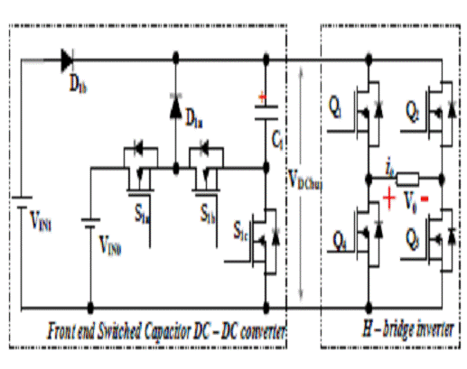
Fig. 1. (a) Single H-Bridge ; (b) Double cascaded H-Bridges.

.
EXPECTED SIMULATION RESULTS


 Fig. 2. (a) and (d) Ch.1:-CHB1, Ch.2:-CHB2, Ch.3:-R1 and Ch.4:-R2; (b) and (e) Ch.1:-VHB1, Ch.2:-VHB2 and Ch.3:-VHB and (c) and (f) Ch.1:-VRO, Ch.2:- VBO and Ch.3:-VYO when (i) the zero crossings of voltage references are in phase with the zero crossings of carrier CHB1 and (ii) the zero crossings of voltage references are placed at the midpoint of the positive zero crossings of carriers CHB1 & CHB2 for fc=3fs with a modulation index of 0.8 and fs=50Hz.


Fig. 3. (a) and (d) Ch.1:-CHB1, Ch.2:-CHB2, Ch.3:-R1 and Ch.4:-R2; (b) and (e) Ch.1:-VHB1, Ch.2:-VHB2 and Ch.3:-VHB and (c) and (f) Ch.1:-VRO, Ch.2:- VBO and Ch.3:-VYO when (i) the zero crossings of voltage references are placed at +π/12rad with respect to the zero crossings of carrier CHB1 for fc=3fs with a modulation index of 0.8 and fs=50Hz and (ii) for fc=160Hz with a modulation index of 0.8 and fs=50Hz.


Fig. 4. (a) and (c) Ch.1:-VRO, Ch.2:-VYO, Ch.3:-VRY and Ch.4:-iR; (b) and (d) Harmonic spectrum of VRY for (i) the zero crossings of voltage references are in phase with the zero crossings of carrier CHB1 and (ii) the zero crossings of voltage references are placed at the midpoint of the positive zero crossings of carriers CHB1 & CHB2 for fc=3fs with a modulation index of 0.8 and fs=50Hz.


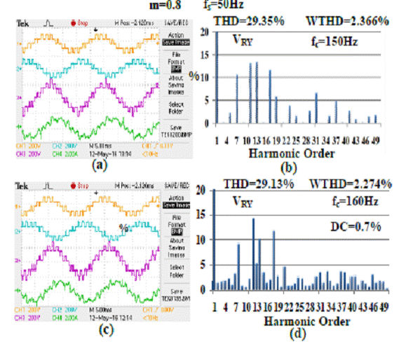
Fig. 5. (a) and (c) Ch.1:-VRO, Ch.2:-VYO, Ch.3:-VRY and Ch.4:-iR; (b) and (d) Harmonic spectrum of VRY for (i) the zero crossings of voltage references are placed at +π/12 rad with respect to the zero crossings of carrier CHB1 for fc=3fs and (ii) fc=160Hz with a modulation index of 0.8 and fs=50Hz.


Fig. 6. (a) Ch.2:- VHB1, Ch.3:- VHB2 and Ch.4:- VHB; (b) Harmonic spectrum of VRO; (c) Ch.1:-VRO, Ch.2:-VYO, Ch.3:-VRY and Ch.4:-iR and (d) Harmonic spectrum of VRY when the zero crossings of voltage references are in phase with the zero crossings of carrier CHB1 for fc=6fs with a modulation index of 0.8 and fs=50Hz.


Fig. 7. (a) Ch.2:- VHB1, Ch.3:- VHB2 and Ch.4:- VHB; (b) Harmonic spectrums of VRO; (c) Ch.1:-VRO, Ch.2:-VYO, Ch.3:-VRY and Ch.4:-iR and (d) Harmonic spectrums of VRY when the zero crossings of voltage references are placed at the midpoint of the zero crossings of carriers CHB1 & CHB2 for fc=6fs with a modulation index of 0.8 and fs=50Hz.


Fig. 8. (a) and (b) Ch.1:-CHB1, Ch.2:-CHB2, Ch.3:-R1 and Ch.4:-R2 and (c) and (d) Ch.1:-VHB1, Ch.2:-VHB2 and Ch.3:-VHB when (i) the zero crossings of voltage references are placed at the midpoint of the positive zero crossings of carriers CHB1 & CHB2 and (ii) the zero crossings of voltage references are in phase with the zero crossings of carrier CHB2 for fc=9fs with a modulation index of 0.9 and fs=45Hz.


Fig. 9. (a) Ch.1:-Transition signal,Ch.2:-CHB1,Ch.3:-CHB2 and Ch.4:-R-Phase voltage reference and (b) Ch.1:-Transition signal,Ch.2:-CHB1,Ch.3:-CHB2 and Ch.4:-iR during the transition from p=9 to p=3.

Fig. 10. (a) and (d) Ch.1:-VHB1, Ch.2:-VHB2, Ch.3:-VHB3 and Ch.4:-VHB4; (b) and (e) Ch.1:-VHB and (c) and (f) Harmonic spectrum of VHB when (i) the positive zero crossing of one carrier co-incides with the zero crossing of fundamental voltage reference and (ii) the zero crossing of fundamental voltage reference is placed at the midpoint of two adjacent carriers with a modulation index of 0.8, fs=50Hz and p=3 for a single phase nine level CHBMLI.

CONCLUSION:
This paper shows analytically the possible positions of zero crossings of the carriers with respect to the zero crossings of voltage references for the CHBMLIs using the PSPWM technique for maintaining three phase symmetry, half wave symmetry and quarter wave symmetry. Three phase and half wave symmetries are maintained among the H-Bridge pole voltage waveforms for any position of zero crossing of carrier with respect to the zero crossing of the voltage references, as long as carrier frequency is 3n time the fundamental frequency with n being any integer (even/odd). But the positions of zero crossings of the carriers with respect to the zero crossings of voltage references are important for maintaining quarter wave symmetry among the pole voltage waveforms. This is analytically studied in this paper for single and two cascaded H-Bridges and generalized for x number of cascaded H-Bridges. The study is experimentally verified with the help of a three phase five level CHBMLI laboratory prototype and the results are presented.
REFERENCES:
[1] J.Rodriguez; S.Bernet; Bin Wu; J.O.Pontt and S.Kouro, ―Multilevel Voltage-Source-Converter Topologies for Industrial Medium-Voltage Drives,‖ IEEE Transactions on Industrial Electronics , vol.54, no.6, pp.2930-2945, Dec. 2007.
[2] H.Abu-Rub; J.Holtz; J.Rodriguez and Ge Baoming, ―Medium-Voltage Multilevel Converters—State of the Art, Challenges, and Requirements in Industrial Applications,‖ IEEE Transactions on Industrial Electronics, vol.57, no.8, pp.2581-2596, Aug. 2010.
[3] S.Kouro; M.Malinowski; K.Gopakumar; J.Pou; L.G.Franquelo; Bin Wu; J.Rodriguez; M.A.Perez and J.L.Leonz   BB  B    , ―Recent Advances and Industrial Applications of Multilevel Converters,‖ IEEE Transactions on Industrial Electronics, vol.57, no.8, pp.2553-2580, Aug. 2010.
[4] G. Narayanan and V.T. Ranganathan, ―Two novel synchronized bus-clamping PWM strategies based on space vector approach for high power drives,‖ IEEE Trans.Power.Electron., vol.17, no.1, pp.84-93,Jan- 2002.
[5] A.R.Beig; S.Kanukollu.;K.Al Hosani and A.Dekka, ―Space-Vector-Based Synchronized Three-Level Discontinuous PWM for Medium-Voltage High-Power VSI‖, IEEE Transactions on Industrial Electronics, vol. 61,no.8,pp. 3891 – 3901, Aug. 2014.


Multi-Input Switched-Capacitor Multilevel Inverter for High-Frequency AC Power Distribution


 ABSTRACT:
This paper proposes a switched-capacitor multilevel inverter for high frequency AC power distribution systems. The proposed topology produces a staircase waveform with higher number of output levels employing fewer components compared to several existing switched capacitor multilevel inverters in the literature. This topology is beneficial where asymmetric DC voltage sources are available e.g. in case of renewable energy farms based AC microgrids and modern electric vehicles. Utilizing the available DC sources as inputs for a single inverter solves the major problem of connecting several inverters in parallel. Additionally, the need to stack voltage sources, like batteries or super-capacitors, in series which demand charge equalization algorithms, are eliminated as the voltage  sources employed share a common ground. The inverter inherently solves the problem of capacitor voltage balancing as each capacitor is charged to the value equal to one of input voltage every cycle. State analysis, losses and the selection of capacitance are examined. Simulation and experimental results at different distribution frequencies, power levels and output harmonic content are provided to demonstrate the feasibility of the proposed multilevel inverter topology.
KEYWORDS:
1.      H-bridge
2.      HFAC power distribution
3.      High frequency DC/AC Inverter
4.      Multilevel inverter
5.      Selective harmonic elimination
6.      Switched-capacitor

SOFTWARE: MATLAB/SIMULINK
CIRCUIT DIAGRAM:


Fig. 1: Proposed 7 level SCMLI topology

 EXPECTED SIMULATION RESULTS


Fig. 2: Simulation waveforms at 400 Hz including nonidealities
: (a) output voltage and current (b) switched capacitor
voltage and current


CONCLUSION:
A novel SCMLI topology for HFAC PDS has been proposed in this paper. The topology is applicable where unequal DC input sources are at disposal. Such scenarios are common in large renewable energy farms and electric vehicle networks. It is more convenient to employ multiple DC sources as input to a single inverter than to employ several inverters in parallel with their respective solitary DC input sources. This topology does not stack up the voltage sources in series and therefore does not require voltage balancing circuits. Since the switched capacitors employed copy the input voltage every cycle, the problem of voltage balancing has also been eliminated. The harmonic content in the waveform is analyzed and is found to be minimum. The proposed topology obtains higher number of voltage levels compared to several existing topologies. This paper utilizes the proposed topology for high frequency AC distribution. However, the same topology can be employed for 50 Hz / 60 Hz distribution by employing a larger switched capacitor. It is shown that the number of output voltage levels exponentially increase with increase in the employed input voltage sources and SCs. In the hardware results, it is shown that the 5th and 7th harmonics are minimized to very low value of 1V each. Results at different distribution frequencies and power levels are presented.
REFERENCES:
[1] Patel, Mukund R.,“High-Power High-Voltage Systems”, Spacecraft Power Systems, CRC press, 2004, ch. 22, sec. 22.7, pp. 539-543.
[2] Luk, Patrick Chi-Kwong, and Andy Seng Yim Ng. ”High Frequency AC Power Distribution Platforms.” Power Electronics in Smart Electrical Energy Networks. Springer London, 2008. pp. 175-201.
[3] Z. Ye, P. K. Jain and P. C. Sen, ”A Two-Stage Resonant Inverter With Control of the Phase Angle and Magnitude of the Output Voltage,” in IEEE Trans. Ind. Electron., vol. 54, no. 5, pp. 2797-2812, Oct. 2007.
[4] J. A. Sabate, M. M. Jovanovic, F. C. Lee and R. T. Gean, ”Analysis and design-optimization of LCC resonant inverter for high-frequency AC distributed power system,” in IEEE Trans. Ind. Electron., vol. 42, no. 1,pp. 63-71, Feb 1995.
[5] Status of 20 kHz Space Station Power Distribution Technology, NASA Publication, TM 100781.

Wednesday 7 November 2018

Modelling, Design, Control, and Implementation of a Modified Z-source Integrated PV/Grid/EVDC Charger/Inverter


ABSTRACT:
Solar Energy has been the most popular sources of renewable energy for residential and semi commercial applications. Fluctuations of solar energy harvested due to atmospheric conditions can be mitigated through energy storage systems. Solar energy can also be used to charge electric vehicle batteries to reduce the dependency on the grid. One of the requirements for a converter for such applications is to have a reduced number of conversion stages and provide isolation. Z-source inverter (ZSI) topology is able to remove multiple stages and achieve voltage boost and DC-AC power conversion in a single stage. The use of passive components also presents an opportunity to integrate energy storage systems (ESS) into them. This paper presents modeling, design and operation of a modified Z-source inverter (MZSI) integrated with a split primary isolated battery charger for DC charging of electric vehicles (EV) batteries. Simulation and experimental results have been presented for the proof of concept of the operation of the proposed converter.
KEYWORDS:
1.      Z-source-inverters
2.      Active filter
3.      Energy storage
4.      Photovoltaic (PV) power generation
5.      Quasi-Zsource inverter (qZSI)
6.      Single-phase systems
7.      Transportation electrification
8.      Solar energy
9.      Distributed power generation
10.  Inverter
SOFTWARE: MATLAB/SIMULINK
BLOCK DIAGRAM:


Fig. 1. Simplified Block Diagram of the System


EXPECTED SIMULATION RESULTS


Fig. 2. Simulation Waveform of the grid current,Ig, DC link voltage,VPN, Capacitor Voltage,VC1, and Battery current,ib for the power balance between the Photovoltaic input power, the AC Grid side and the battery power.


Fig. 3. Simulation Waveform for the power balance between the Photovoltaic input power, the AC Grid side and the battery power.


CONCLUSION:
A modified ZSI topology has been proposed in this paper is an attractive solution for photovoltaic grid connected charging systems. It consist of a single stage photovoltaic grid (PV-Grid) connection and an integrated charger for PV-Grid connected charging or energy storage. This topology can be applied to centralized configuration for charging in semi-commercial locations such as a parking lot of a shopping mall. For residential applications, this idea can be extended to string inverters with the charger side of the string inverter configurations connected in series or parallel for current sharing. The paper proposes a an energy storage topology using Z source converter through symmetrical operation of its impedance network.
REFERENCES:
[1] D. Aggeler, F. Canales, H. Zelaya, D. L. Parra, A. Coccia N. Butcher, and O. Apeldoorn, “Ultra-fast dc-charge infrastructures for ev-mobility and future smart grids,” in Proc. of IEEE PES Innovative Smart Grid Technologies Conference Europe, pp. 1–8, Oct. 2010.
[2] G. Carli and S. S. Williamson, “Technical considerations on power conversion for electric and plug-in hybrid electric vehicle battery charging in photovoltaic installations,” IEEE Trans. on Ind. Electron., vol. 28, no. 12, pp. 5784–5792, 2013.
[3] J. G. Ingersoll and C. A. Perkins, “The 2.1 kw photovoltaic electric vehicle charging station in the city of santa monica, california,” in Proc. of the Twenty Fifth IEEE Photovoltaic Specialists Conference, pp. 1509– 1512, May. 1996.
[4] S. B. Kjaer, J. K. Pedersen, and F. Blaabjerg, “A review of single-phase grid-connected inverters for photovoltaic modules,” IEEE Trans. on Ind. Appl., vol. 41, no. 5, pp. 1292–1306, Sep. 2005.
[5] N. A. Ninad, L. A. C. Lopes, and I. S. Member, “Operation of Single-phase Grid-Connected Inverters with Large DC Bus Voltage Ripple,” Proc. of the IEEE Canada Electrical Power Conference, 2007.


UDE-Based Current Control Strategy for LCCL-Type Grid-Tied Inverters


ABSTRACT:
LCL filter is usually used as an interface between inverters and the grid. However, due to the characteristics of LCL filter and system uncertainties, it is complex to design a controller with proper parameters. In this paper, with LCCL filter, the order of the inverter control system can be reduced from third order to first order, and an uncertainty and disturbance estimator based control strategy for grid-tied inverters with LCCL filter is proposed. Specifically, the proposed control strategy consists of differential feed forward, proportional–integral controller, and grid voltage feed forward. Moreover, with one-sampling computation plus half-sampling pulse width modulation delays considered, a simple and clear tuning algorithm for the proposed control strategy is presented. Finally, the inverter system with the proposed control strategy is investigated, and the effectiveness is supported by the tuning and comparative experiments with a 2-kW inverter.
KEYWORDS:
1.      Current control
2.      Inverter
3.      LCCL filter
4.      Tuning  algorithm
5.      Uncertainty and disturbance estimator (UDE)

 SOFTWARE: MATLAB/SIMULINK

CIRCUIT DIAGRAM:


Fig. 1. System topology of the grid-tied inverter with LCCL filter.

.
EXPECTED SIMULATION RESULTS


Fig. 2. Result of UDE-based control without grid voltage feed forward. (a) Injected grid current i2 . (b) Spectrum of the injected grid current.


Fig. 3. Tuning results of UDE-based control with the same α = 10 000 rad/s, β = 5000 rad/s, and different k. (a) k = 10 000 rad/s. (b) k = 9000 rad/s. (c) k = 7000 rad/s.

Fig. 4. Result of UDE-based control under i*12 (s) = 10 A with α = 10 000 rad/s, β = 5000 rad/s, and k = 8000 rad/s. (a) Injected grid current i2 . (b) Spectrum of the injected grid current.


Fig. 5. Result of PI control under i*12 (s) = 10 A with kp = 17 and ki  = 14400. (a) Injected grid current i2 . (b) Spectrum of the injected grid current.


CONCLUSION:
For grid-tied inverter, LCL filter is widely used to attenuate the high switching frequency harmonics caused by PWM. However, due to the characteristic of LCL filter and uncertainty, it is complex to design a controller with proper parameters. In this paper, with LCCL filter, the inverter control system can be degraded from third order to first order. And a UDE-based injected grid current control strategy was built. The proposed strategy unified the system uncertainty and disturbance into the lumped disturbances, and the closed-loop system adjusted by PI regulator approached to the reference model. Meanwhile, the PI controller can be expressed in the error feedback gain, the desired closed-loop bandwidth, and the approximate lumped disturbance bandwidth. Moreover, with one-sampling computation plus half-sampling PWM delays considered, a simple and clear tuning algorithm for the proposed control strategy was provided. Finally, the proposed strategy was verified by the tuning and comparative experiments on a 2-kW inverter.
REFERENCES:

 [1] M. Lindgren and J. Svensson, “Control of a voltage-source converter connected to the grid through an LCL-filter-application to active filtering,” in Proc. IEEE Power Electron. Spec. Conf., May 1998, pp. 229–235.
[2] E. Twining and D. G. Holmes, “Grid current regulation of a three-phase voltage source inverter with an LCL input filter,” IEEE Trans. Power Electron., vol. 18, no. 3, pp. 888–895, May 2003.
[3] G. Shen, D. Xu, L. Cao, and X. Zhu, “An improved control strategy for grid-connected voltage source inverters with an LCL filter,” IEEE Trans. Power Electron., vol. 23, no. 4, pp. 1899–1906, Jul. 2008.
[4] G. Shen, X. Zhu, J. Zhang, and D. Xu, “A new feedback method for PR current control ofLCL-filter-based grid-connected inverter,” IEEE Trans. Ind. Electron., vol. 57, no. 6, pp. 2033–2041, Jun. 2010.
[5] R. P. Alzola, M. Liserre, F. Blaabjerg, R. Sebasti´an, J. Dannehl, and F. W. Fuchs, “Analysis of the passive damping losses in LCL-filter-based grid converters,” IEEE Trans. Power Electron., vol. 28, no. 6, pp. 2642–2646, Jun. 2013.