ABSTRACT:
This paper analyses synchronization strategy for
cascaded H-Bridge multi level inverter (CHBMLI) topologies with carrier based
sinusoidal phase shifted pulse width modulation (PSPWM) technique. In PSPWM
technique a separate carrier is used for each H-Bridge (HB). The carriers are
generally phase shifted from each other by π/x rad (x=No. of H-Bridges) for
unipolar PWM. With the carrier frequency being an integer (odd/even) multiple
of the fundamental frequency, it is observed that, the positions of zero
crossings of the carriers with respect to the zero crossings of voltage
references play an important role for maintaining quarter wave symmetry among
multi level inverter (MLI) pole voltage waveforms. This paper analytically
shows the conditions for half wave symmetry and quarter wave symmetry and
experimentally verifies those conditions for PSPWM technique with a five level
CHBMLI laboratory prototype.
KEYWORDS:
1. Cascaded H-Bridge multilevel inverter
2. Phase shifted carrier based PWM
3. Synchronous PWM
4. Half wave symmetry
5. Quarter wave symmetry
SOFTWARE: MATLAB/SIMULINK
Fig. 1. (a) Single H-Bridge ; (b) Double cascaded H-Bridges.
.
EXPECTED SIMULATION RESULTS
Fig. 3. (a) and (d) Ch.1:-CHB1, Ch.2:-CHB2, Ch.3:-R1 and Ch.4:-R2; (b)
and (e) Ch.1:-VHB1, Ch.2:-VHB2 and Ch.3:-VHB and (c) and (f) Ch.1:-VRO, Ch.2:-
VBO and Ch.3:-VYO when (i) the zero crossings of voltage references are placed
at +π/12rad with respect to the zero crossings of carrier CHB1 for fc=3fs with
a modulation index of 0.8 and fs=50Hz and (ii) for fc=160Hz with a modulation
index of 0.8 and fs=50Hz.
Fig. 4. (a) and (c) Ch.1:-VRO, Ch.2:-VYO, Ch.3:-VRY and Ch.4:-iR; (b)
and (d) Harmonic spectrum of VRY for (i) the zero crossings of voltage
references are in phase with the zero crossings of carrier CHB1 and (ii) the
zero crossings of voltage references are placed at the midpoint of the positive
zero crossings of carriers CHB1 & CHB2 for fc=3fs with a modulation index
of 0.8 and fs=50Hz.
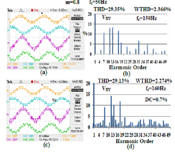
Fig. 5. (a) and (c) Ch.1:-VRO, Ch.2:-VYO, Ch.3:-VRY and Ch.4:-iR; (b)
and (d) Harmonic spectrum of VRY for (i) the zero crossings of voltage references
are placed at +π/12 rad with respect to the zero crossings of carrier CHB1 for
fc=3fs and (ii) fc=160Hz with a modulation index of 0.8 and fs=50Hz.
Fig. 6. (a) Ch.2:- VHB1, Ch.3:- VHB2 and Ch.4:- VHB; (b) Harmonic
spectrum of VRO; (c) Ch.1:-VRO, Ch.2:-VYO, Ch.3:-VRY and Ch.4:-iR and (d)
Harmonic spectrum of VRY when the zero crossings of voltage references are in
phase with the zero crossings of carrier CHB1 for fc=6fs with a modulation
index of 0.8 and fs=50Hz.
Fig. 7. (a) Ch.2:- VHB1, Ch.3:- VHB2 and Ch.4:- VHB; (b) Harmonic
spectrums of VRO; (c) Ch.1:-VRO, Ch.2:-VYO, Ch.3:-VRY and Ch.4:-iR and (d)
Harmonic spectrums of VRY when the zero crossings of voltage references are
placed at the midpoint of the zero crossings of carriers CHB1 & CHB2 for
fc=6fs with a modulation index of 0.8 and fs=50Hz.
Fig. 8. (a) and (b) Ch.1:-CHB1, Ch.2:-CHB2, Ch.3:-R1 and Ch.4:-R2 and
(c) and (d) Ch.1:-VHB1, Ch.2:-VHB2 and Ch.3:-VHB when (i) the zero crossings of
voltage references are placed at the midpoint of the positive zero crossings of
carriers CHB1 & CHB2 and (ii) the zero crossings of voltage references are
in phase with the zero crossings of carrier CHB2 for fc=9fs with a modulation
index of 0.9 and fs=45Hz.
Fig. 9. (a) Ch.1:-Transition signal,Ch.2:-CHB1,Ch.3:-CHB2 and
Ch.4:-R-Phase voltage reference and (b) Ch.1:-Transition
signal,Ch.2:-CHB1,Ch.3:-CHB2 and Ch.4:-iR during the transition from p=9 to
p=3.
Fig. 10. (a) and (d) Ch.1:-VHB1, Ch.2:-VHB2, Ch.3:-VHB3 and Ch.4:-VHB4;
(b) and (e) Ch.1:-VHB and (c) and (f) Harmonic spectrum of VHB when (i) the
positive zero crossing of one carrier co-incides with the zero crossing of
fundamental voltage reference and (ii) the zero crossing of fundamental voltage
reference is placed at the midpoint of two adjacent carriers with a modulation
index of 0.8, fs=50Hz and p=3 for a single phase nine level CHBMLI.
CONCLUSION:
This
paper shows analytically the possible positions of zero crossings of the
carriers with respect to the zero crossings of voltage references for the
CHBMLIs using the PSPWM technique for maintaining three phase symmetry, half
wave symmetry and quarter wave symmetry. Three phase and half wave symmetries
are maintained among the H-Bridge pole voltage waveforms for any position of zero
crossing of carrier with respect to the zero crossing of the voltage
references, as long as carrier frequency is 3n time the fundamental frequency
with n being any integer (even/odd). But the positions of zero crossings of the
carriers with respect to the zero crossings of voltage references are important
for maintaining quarter wave symmetry among the pole voltage waveforms. This is
analytically studied in this paper for single and two cascaded H-Bridges and
generalized for x number of cascaded H-Bridges. The study is experimentally
verified with the help of a three phase five level CHBMLI laboratory prototype
and the results are presented.
REFERENCES:
[1] J.Rodriguez;
S.Bernet; Bin Wu; J.O.Pontt and S.Kouro, ―Multilevel Voltage-Source-Converter
Topologies for Industrial Medium-Voltage Drives,‖ IEEE Transactions on
Industrial Electronics , vol.54, no.6, pp.2930-2945, Dec. 2007.
[2]
H.Abu-Rub; J.Holtz; J.Rodriguez and Ge Baoming, ―Medium-Voltage Multilevel
Converters—State of the Art, Challenges, and Requirements in Industrial
Applications,‖ IEEE Transactions on Industrial Electronics, vol.57,
no.8, pp.2581-2596, Aug. 2010.
[3]
S.Kouro; M.Malinowski; K.Gopakumar; J.Pou; L.G.Franquelo; Bin Wu; J.Rodriguez;
M.A.Perez and J.L.Leonz BB B ,
―Recent Advances and Industrial Applications of Multilevel Converters,‖ IEEE
Transactions on Industrial Electronics, vol.57, no.8, pp.2553-2580, Aug.
2010.
[4] G. Narayanan
and V.T. Ranganathan, ―Two novel synchronized bus-clamping PWM strategies based
on space vector approach for high power drives,‖ IEEE Trans.Power.Electron.,
vol.17, no.1, pp.84-93,Jan- 2002.
[5] A.R.Beig;
S.Kanukollu.;K.Al Hosani and A.Dekka, ―Space-Vector-Based Synchronized
Three-Level Discontinuous PWM for Medium-Voltage High-Power VSI‖, IEEE
Transactions on Industrial Electronics, vol. 61,no.8,pp. 3891 – 3901, Aug.
2014.


