asokatechnologies@gmail.com 09347143789/09949240245

Search This Blog

Sunday 5 January 2020

Design of a PEV Battery Charger with High Power Factor using Half-bridge LLC-SRC Operating at Resonance Frequen


ABSTRACT:
This paper presents a two stage battery charger for plug-in electric vehicles (PEV) based on half-bridge LLC series resonant converter (SRC) operating at resonance frequency. The first stage is power factor correction (PFC) stage comprising of boost converter topology using hysteresis band control of inductor current. The PFC stage reduces the total harmonic distortion (THD) of the line current for achieving high power factor and regulates the voltage to follow the battery voltage at DC link capacitor. The input of the boost converter is a single phase 50 Hz, 220V AC from grid. At the second stage, a half bridge LLC-SRC is used for constant-current, constant-voltage (CC-CV) based battery charging and for providing galvanic isolation. The resonant converter is designed to operate around resonance frequency to have maximum efficiency and low turnoff current of power switches to reduce switching losses. The circuit is simulated using MATLAB Simulink with 1.5 Kw maximum output power. Simulation results show that the PFC  stage achieves THD less than 0.07% and high power factor value  as 0.9976. The DC/DC stage meets all the CC-CV charging requirements of the battery over wide voltage range 320V—420V for depleted to fully charged battery.
KEYWORDS:
1.      LLC Resonant converter
2.      PEV battery charger
3.      PFC
4.      Hysteresis band control
5.      FHA
SOFTWARE: MATLAB/SIMULINK

BLOCK DIAGRAM:

Fig.1. Typical power architecture of a battery charger.

CIRCUIT DIAGRAM:


Fig. 2. Schematic of the proposed battery charger.
EXPERIMENTAL RESULTS:


Fig. 3. Boost inductor current for a half cycle of input voltage.


Fig. 
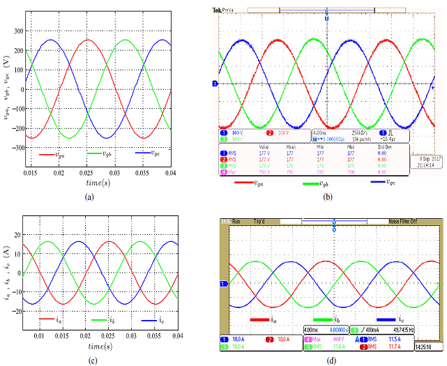
4. AC voltage and current after power factor correction.


Fig. 5. LLC-SRC operating at key point A (V0 = 320V, and I0 = 3.57A).
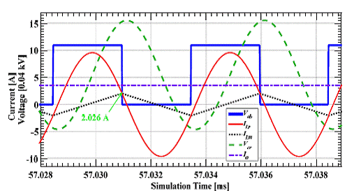


Fig. 6. LLC-SRC operating at key point B (V0 = 360V, and I0 = 3.57A).


Fig. 7. LLC-SRC operating at key point C (V0 = 420V, and I0 = 3.57A).


Fig. 8. LLC-SRC operating at key point D (V0 = 420V, and I0 = 0.25A).


CONCLUSION:
In this paper, a 1.5 kW PEV battery charger with emphasis on the design of LLC-SRC for DC-DC stage of the battery charger is presented. A method for improvement in the power  factor with boost converter is presented using hysteresis current control to keep line input voltage and current in phase using  phase shift in inductor current. Simulation results show that the PFC stage achieves minimum THD as 0.07% and a power factor of 0.9976 having line current and voltage in phase. The LLC-SRC is designed to operate around resonance frequency to achieve maximum benefits of LLC converter,  having minimum circulating energy, avoiding hard  commutation of secondary rectifier diodes. Simulation results for the converter performance are presented which show that the turning off current of power switches have very low value throughout the charging process and is below 2.4A. Hence, the converter have minimum switching and conduction losses.
REFERENCES:
[1] H. Wang, S. Dusmez, and A. Khaligh, "A novel approach to design EV battery chargers using SEPIC PFC stage and optimal operating point tracking technique for LLC converter," Applied Power Electronics Conference and Exposition (APEC), 2014 Twenty-Ninth Annual IEEE, pp.1683-1689, 16-20 March 2014.
[2] H. Wang, S. Dusmez, and A. Khaligh, "Design and Analysis of a Full-Bridge LLCBased  PEV Charger Optimized for Wide Battery Voltage Range," Vehicular Technology, IEEE Transactions on, Vol. 63, No. 4, pp.1603-1613, May 2014.
[3] J. Deng, S. Li, S. Hu, C.C. Mi, and R. Ma, "Design Methodology of LLC Resonant Converters for Electric Vehicle Battery Chargers," Vehicular Technology, IEEE Transactions on, Vol. 63, No. 4, pp.1581-1592, May 2014.
[4] Marian K. Kazimierczuk, "Pulse-width Modulated DC-DC Power Converters," Ohio, USA: John Wiley & Sons Ltd, pp. 129-134, 2008.
[5] H. Wang, and A. Khaligh, "Comprehensive Topological Analyses of Isolated Resonant Converters in PEV Battery Charging Applications," Transportation Electrification Conference and Expo (ITEC), 2013 IEEE, pp.1-7, 16-19 June 2013.

Saturday 28 December 2019

Improved pulse-width modulation scheme for T-type multilevel inverter


ABSTRACT: 

In recent times, reduced switch count multilevel inverter (RSC-MLI) has become an emerging area of research in power electronic converters. To control these RSC-MLI topologies, various novel modulation schemes are reported. Multi reference is one of such modulation scheme reported for various RSC topologies, such as T-type. However, the performance of this conventional scheme results in high total harmonic distortion (THD) in line voltages, when compared with the conventional level shifted pulse-width modulation scheme. This observation is clearly presented in this study and the reason for its degraded THD performance has been deeply discussed. To alleviate this problem, a modified multi-reference dual-carrier modulation technique with multiple references and two carriers is proposed. To implement this proposed modulation technique, an alternate carrier and modulation signals arrangement with multiple carriers and single reference is also presented. Finally, a comparative THD performance of the proposed and conventional modulation schemes is carried out on a five-level T-type MLI and obtained simulation results are validated experimentally.

SOFTWARE: MATLAB/SIMULINK

CIRCUIT DIAGRAM:


Fig. 1 Five-level T-type topology

EXPERIMENTAL RESULTS: 


Fig. 2 Performance analysis of multi-reference modulation scheme on five-level T-type configuration with ma = 0.95 and fc = 1500 Hz (a) Phase voltage, line voltage and load current, (b) Respective harmonic spectra, (c) Comparative harmonic performance of conventional multi-reference modulation scheme for five-level T-type MLI and LSPWM for five-level CHB


Fig. 3 Comparison of LSPWM-OPD and multi-reference modulation scheme with ma = 0.95 and fc = 1500 Hz
(a) Conventional multi-reference modulation scheme for a five-level T-type, (b) Comparison of position of carriers in multi-reference modulation in terms of LSPWM-OPD scheme,
(c) Position of carriers in LSPWM-OPD modulation scheme, (d) Phase and line harmonic spectra of LSPWM-OPD for a five-level CHB


Fig. 4 Modified multi-reference dual-carrier modulation scheme for a five-level T-type topology with ma = 0.95 and fc = 1500 Hz (a) Proposed scheme, (b) Carriers of proposed scheme in terms of LSPWM-IPD, (c) Phase voltage, line voltage and load current, (d) Respective harmonic spectra

CONCLUSION:

In this paper, the poor harmonic performance of the conventional multi-reference modulation method for T-type MLI topology is analysed. To address this problem, a modified multi-reference dual-carrier modulation is proposed. The performance of the proposed modulation scheme is identical to LSPWM-IPD technique which is the best PWM technique with lowest THD value available. Further, to implement the proposed PWM scheme, an alternate carrier and modulation signals arrangement is also proposed which can be easily realisable on digital platforms. The performance of the proposed modulation schemes is evaluated with simulation and experimental studies on a five-level T-type MLI topology. The experimental studies are in good agreement with simulation studies and also verify the superior performance of the proposed schemes over conventional modulation schemes. A generalisation of the modified reduced carrier modulation to implement any number of levels for a T-type is presented with the help of a flowchart.

REFERENCES:

[1] Singh, B., Singh, B.N., Chandra, A., et al.: ‘A review of three-phase improved power quality AC–DC converters’, IEEE Trans. Ind. Electron., 2004, 51, (3), pp. 641–660
[2] Franquelo, L.G., Rodriguez, J., Leon, J.I., et al.: ‘The age of multilevel converters arrives’, IEEE Ind. Electron. Mag., 2008, 2, (2), pp. 28–39
[3] Kouro, S., Malinowski, M., Gopakumar, K., Pou, J., Franquelo, L.G., Wu, B., Rodriguez, J., Pérez, M.A., Leon, J.I.: ‘Recent advances and industrial applications of multilevel converters’, IEEE Trans. Ind. Electron., 2010, 57, (8), pp. 2553–2580
[4] Rodriguez, J., Lai, J.-S., Peng, F.Z.: ‘Multilevel inverters: a survey of topologies, controls, and applications’, IEEE Trans. Ind. Electron., 2002, 49, (4), pp. 724–738, doi: 10.1109/TIE.2002.801052
[5] McGrath, B.P., Holmes, D.G.: ‘Multicarrier PWM strategies for multilevel inverters’, IEEE Trans. Ind. Electron., 2002, 49, (4), pp. 858–867

Tuesday 17 December 2019

Vector Current Control Derived from Direct Power Control for Grid-Connected Inverters


ABSTRACT:
We propose a vector current control derived from direct power control (VCC-DPC) for a three-phase voltage source inverter (VSI) in the synchronous rotating frame through instantaneous real and reactive powers. The proposed VCC-DPC method has the same control structure as the conventional VCC except for the coordinate transformation, since we obtain the d–q axes currents model of VSI without using Park transformation  and the PLL system. Consequently, the proposed method has the same property as the conventional VCC if the PLL extracts the phase angle of the grid voltage correctly. However, with the consideration of the slow dynamics of the PLL, the proposed method has an enhanced dynamical performance feature compared with the conventional VCC. Moreover, it has another benefit that the reduction of the computational burden could be expected since  there is no Park transformation and the PLL in the controller implementation. We can guarantee that the closed-loop system with the proposed method is exponentially stable in the operating  range. Finally, both simulation and experimental results using a 15-kW-inverter system match the theoretical expectations closely.
KEYWORDS:
1.      Voltage source inverter
2.      Vector current controller
3.      Instantaneous real and reactive powers
4.      Exponentially stable

SOFTWARE: MATLAB/SIMULINK

 BLOCK DIAGRAM:


Fig. 1. Block diagram of (a) the standard VCC with PLL; (b) the proposed method without PLL.

EXPERIMENTAL RESULTS:


Fig. 2. Performance of the inverter when the reference of id is changed from 5 A to 10 A at 1:51 s. (a) grid voltage, (b) id, (c) iq. (red-solid line: conventional method; blue-dashed line: proposed method).


Fig. 3. Performance of the inverter when the inverter is connected at 0:51 s and the reference of id is changed to 5 A. (a) grid voltage, (b) real power, (c) reactive power, (d) id, (e) iq, (red-solid line: conventional VCC method; green-solid line: conventional VCC method with faster PLL; blue-dashed line: proposed method)

CONCLUSION:
In this paper, we have introduced a VCC-DPC for three phase VSI with instantaneous real and reactive powers. We obtained the d–q axes currents model of VSI without using Park transformation and the PLL. For fair comparison, we designed a PI controller with feed forward. Thus, the proposed method has the same control structure as the conventional VCC except for the coordinate transformation and PLL. Moreover, the proposed VCC-DPC will reduce the computational burden since there is no Park transformation and as well as the PLL. Simulation results show that the proposed method has the same properties as the conventional VCC when the PLL extracts the correct phase angle of the grid voltage. However, in the case where the slow dynamics of the PLL is activated,   the proposed method has improved dynamical performance in  comparison with the conventional VCC. We have also tested the performance of the proposed method with a 15-kW inverter system. Experimental results show that the proposed method has a robust property for the parameter uncertainness as well. This work is an initial start for the VCC-DPC through the DPC model. In the future, we will design a compensator for the harmonics or unbalanced issues based on this concept.
REFERENCES:
[1] F. Blaabjerg, R. Teodorescu, M. Liserre, and A. V. Timbus, “Overview of control and grid synchronization for distributed power generation systems,” IEEE Trans. Ind. Electron., vol. 53, no. 5, pp. 1398–1409, 2006.
[2] F. Blaabjerg, M. Liserre, and K. Ma, “Power electronics converters for wind turbine systems,” IEEE Trans. Ind. Appl., vol. 48, no. 2, pp. 708–  719, 2012.
[3] F. Blaabjerg, Y. Yang, D. Yang, and X. Wang, “Distributed power generation  systems and protection,” Proc. IEEE, vol. 105, no. 7, pp. 1311–1331, 2017.
[4] Q.-C. Zhong, “Power-electronics-enabled autonomous power systems: Architecture and technical routes,” IEEE Trans. Ind. Electron., vol. 64, no. 7, pp. 5907–5918, 2017.
[5] X. Wang, F. Blaabjerg, M. Liserre, Z. Chen, J. He, and Y. Li, “An active damper for stabilizing power-electronics-based AC systems,”  IEEE Trans. Power Electron., vol. 29, no. 7, pp. 3318–3329, 2014.

Three Phase Single Stage Isolated Cuk based PFC Converter


ABSTRACT:
 In this paper, analysis and design of a three phase isolated Cuk based power factor correction (PFC) converter has been proposed. The proposed converter is operated in discontinuous output inductor current mode (DOICM) to achieve PFC at ac input. This avoids the inner current control loop which further eliminates the sensing of current. This makes the system more reliable and robust. The converter requires only one simple voltage control loop for output voltage regulation and all the power switches are driven by the same gate signal which simplifies the gate driver circuit. The detailed operation of the converter and design calculations are presented. And also a small signal model of the converter by using CIECE approach is presented to aid the controller design. The experimental results from a 2-kW laboratory prototype with 208-V line-to-line input voltage, 400-V output voltage are presented to confirm the operation of the proposed converter. An input power factor of 0.999, an input current total harmonic distortion of as low as 4.06% and a high conversion efficiency of 95.1% are achieved from laboratory prototype.
KEYWORDS:
1.      Three phase power factor correction (PFC)
2.      Isolation
3.      Cuk converter
4.      Discontinuous conduction mode (DCM)
5.      AC-DC converters

SOFTWARE: MATLAB/SIMULINK

CIRCUIT DIAGRAM:


Fig. 1. (a) Single phase isolated Cuk PFC converter; (b) Proposed structure of the three phase isolated Cuk converter.


EXPERIMENTAL RESULTS:


Fig. 2. Experimental waveforms at 1kW output power: (a) input voltages of each phase (50V/div); (b) input currents of each phase and output voltage (2.0A/div, 200V/div); (c) input voltage (50V/div) and input current (2.0A/div) of each phase; (d) input current harmonic spectrum.


Fig.3. Experimental waveforms at 1kW output power: (a) input voltage and voltage across capacitor 𝑐1𝑎 (100V/div); (b) output voltage and voltage across capacitor 𝑐2𝑎 (100V/div); (c) one phase transformer primary and secondary currents (5.0A/div each); (d) output currents of each module (5.0A/div); (e) transformer primary voltages of each phase (200V/div); (f) voltage across each switch (200V/div).


Fig. 4. (a) The experimental output voltage (200V/div), output current (2.0A/div) and input current (5.0A/div) for load power disturbance from 0.8 kW to 1.0 kW; (b) The experimental output voltage (100V/div), input voltage (100V/div) and input current (5.0A/div) for phase input voltage disturbance from 100 V to 115 V.


CONCLUSION:
In this paper, a three phase isolated Cuk converter based power factor correction rectifier operating in discontinuous output inductor current mode (DOICM) is presented. Due to the large size input inductor filter, the proposed converter does not require an additional input filter. The steady state operation of the converter and each component design have been given in detail. It is shown that by operating the converter in DOICM, the input currents are sinusoidal and in phase with input voltages. Subsequently, it does not require inner current control loop and eliminates the current sensors which reduces the system cost and increase the reliability. Another advantage is that the converter works with zero current turn off in the output diode which eliminates the reverse recovery losses of diodes. To aid the controller design, detailed small signal model of the converter by using CIECE approach is presented. A simple voltage control loop with only one output voltage sensor is used to regulate the output voltage.
An experimental laboratory prototype of 2 kW is designed and built to confirm the operation of the proposed converter. The experimental results confirms the analysis and operation of the converter. A high efficiency of 95.1% and an input current THD as low as 4.06% are achieved with the developed laboratory prototype.

REFERENCES:

[1] Limits for Harmonic Current Emissions (Equipment Input Current <16A Per Phase), IEC/EN61000-3-2, 1995.
[2] IEEE Recommended Practices and Requirements for Harmonics Control in Electric Power Systems, IEEE Std. 519, 1992.
[3] D. Gauger, T. Froeschle, L. Illingworth and E. Rhyne, "A Three-Phase Off-Line Switching Power Supply with Unity Power Factor and Low TIF," Telecommunications Energy Conference, 1986. INTELEC '86. International, Toronto, Canada, 1986, pp. 115-121.
[4] BREWSTER, R.F., and BARRET, A.H., “Three-phase AC to DC voltage converter with power line harmonic current reduction,” US Patent 4143414, 6th March, 1979.
[5] D. Chapman, D. James and C. J. Tuck, "A high density 48 V 200 A rectifier with power factor correction-an engineering overview," Proceedings of Intelec 93: 15th International Telecommunications Energy Conference, Paris, 1993, vol. 1, pp. 118-125.


Monday 16 December 2019

A Unidirectional Single-Stage Three-Phase Soft-switched Isolated DC-AC Converter


ABSTRACT:
This paper presents a novel single-stage soft switched high frequency link three-phase DC-AC converter topology. The topology supports unidirectional DC to AC power flow and is targeted for applications like grid integration of photovoltaic sources, fuel cell etc. The high frequency magnetic isolation results in reduction of system volume, weight and cost. Sine-wave pulse width modulation is implemented in DC side converter. Though high frequency switched, DC side converter is soft-switched for most part of the line cycle. The AC side converter active switches are line frequency switched incurring negligible switching loss. The line frequency switching of AC side converter facilitates use of high voltage blocking inherently slow semiconductor devices to generate high voltage AC output. In addition, a cascaded multilevel structure is presented in this paper for direct medium voltage AC grid integration. A detailed circuit analysis considering non-idealities like transformer leakage and switch capacitances, is presented in this paper. A 6kW three phase laboratory prototype is build. The presented simulation and experimental results verify the operation of proposed topologies.
KEYWORDS:
1.      Zero-voltage switching (ZVS)
2.      Pulse width modulation
3.      DC-AC converter
4.      High-frequency transformer (HFT)
5.      Cascaded multilevel inverter
6.      Single-stage
7.      Rectifier-type HFL
SOFTWARE: MATLAB/SIMULINK
CIRCUIT DIAGRAM:


Fig. 1. Proposed 3φ single stage HFL topology

Fig. 2. Proposed 3φ cascaded multilevel HFL topology

EXPERIMENTAL RESULTS:


Fig. 3. Output phase voltages- (a) simulation, (b) experimental: [CH1] c phase voltage (100V/div.), [CH2] a phase voltage (100V/div.), [CH3] b phase voltage (100V/div.). Time scale 4ms/div. Output current waveforms- (c) simulation, (d) experimental: [CH1] c phase current (10A/div.), [CH2] a phase current (10A/div.), [CH3] b phase current (10A/div.). Time scale 4ms/div.

CONCLUSION:
In this paper, a single-stage unidirectional 3φ high frequency link inverter topology along with its multilevel configuration is proposed. Proposed topologies have following features. 1) The DC side converter is soft switched (ZVS) for most part of the line cycle without additional snubber circuit.  2) High frequency magnetic isolation improves the system power density and reduces weight and cost. 3) The AC side active switches are line frequency switched incurring negligible switching loss. 4) High voltage blocking slow switches can be used in line frequency switched AC side converter to generate high voltage AC output. 5) The cascaded structure proposed in this paper is targeted for direct medium voltage grid integration and 6) in this scheme the grid end line filter will have high voltage and low current rating resulting in smaller size with reduced conduction loss. The circuit operation of the proposed converters are discussed in detail considering non-idealities like transformer leakage inductance and device capacitances. The presented simulation and experimental results at verify the operation principle and advantages of the proposed converter topologies. The proposed topologies support unidirectional DC to AC power flow and primarily targeted for grid integration of utility scale photovoltaic sources.

REFERENCES:
[1] J. M. Carrasco, L. G. Franquelo, J. T. Bialasiewicz, E. Galv´an, R. C. PortilloGuisado, M. M. Prats, J. I. Le´on, and N. Moreno-Alfonso, “Power-electronic systems for the grid integration of renewable energy sources: A survey,” IEEE Transactions on industrial electronics, vol. 53, no. 4, pp. 1002–1016, 2006.
[2] E. Romero-Cadaval, G. Spagnuolo, L. G. Franquelo, C. A. Ramos-Paja, T. Suntio, and W. M. Xiao, “Grid-connected photovoltaic generation plants: Components and operation,” IEEE Industrial Electronics Magazine, vol. 7, no. 3, pp. 6–20, 2013.
[3] S. Essakiappan, H. S. Krishnamoorthy, P. Enjeti, R. S. Balog, and  S. Ahmed, “Multilevel medium-frequency link inverter for utility scale  photovoltaic integration,” IEEE Transactions on Power Electronics,  vol. 30, no. 7, pp. 3674–3684, 2015.
[4] Y. Shi, R. Li, Y. Xue, and H. Li, “High-frequency-link-based grid tied pv system with small dc-link capacitor and low-frequency ripple free maximum power point tracking,” IEEE Transactions on Power Electronics, vol. 31, no. 1, pp. 328–339, 2016.
[5] K. V. Iyer, R. Baranwal, and N. Mohan, “A high-frequency ac-link single-stage asymmetrical multilevel converter for grid integration of renewable energy systems,” IEEE Transactions on Power Electronics, vol. 32, no. 7, pp. 5087–5108, 2017.