ABSTRACT
The
aim of this study is to present a new structure for switched-capacitor
multilevel inverters (SCMLIs) which can generate a great number of voltage
levels with optimum number of components for both symmetric and asymmetric
value of dc voltage sources. Proposed topology consists of a new
switched-capacitor dc/dc converter (SCC) which has boost ability and can charge
capacitors as self-balancing by using proposed binary asymmetrical algorithm
and series-parallel conversion of power supply. Proposed SCC unit is used in
new configuration as a sub-multilevel inverter (SMLI) and then, these proposed
SMLIs are cascaded together and create a new cascaded multilevel inverter
topology which is able to increase the number of output voltage levels
remarkably without using any full H-bridge cell and also can pass the reverse
current for inductive loads. In this case, two half bridges modules besides two
additional switches are employed in each of SMLI units instead of using a full
H-bridge cell which contribute to reduce the number of involved components in
the current path, value of blocked voltage, the variety of isolated dc voltage
sources and as a result the overall cost by less number of switches in
comparison with other presented topologies. The validity of the proposed SCMLI
has been carried out by several simulation and experimental results.
KEYWORDS
1. Cascade sub-multilevel inverter
2. Series-parallel conversion
3. Self-charge
balancing
4. Switched-capacitor
SOFTWARE:
MATLAB/SIMULINK
CIRCUIT DIAGRAM:
Fig.
1. Proposed 17-level structure
EXPECTED SIMULATION RESULTS
(a)
(b)
Fig. 2. Steady states output voltage and current waveforms (a) in
simulation Fig. 12. Transient states of output waveforms in simulation (b)
in experiment ( 250V/div& 2A/div)
Fig.
3. Transient states of output waveforms in simulation
(a) (b)
Fig.
4. Harmonic orders (a) output voltage (b) output current in simulation
Fig. 5. Observed output voltage waveform at no-load condition
(250V/div)
(a)
(b)
Fig.
6. Capacitors’ voltage ripple waveforms for first case study (a) in simulation
(b) in experiment (25 V/dev&50V/div)
Fig.
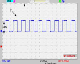
7. Blocked voltage waveforms across switches of S1 (25V/div), S2
(100V/div), T1 (50V/div), T2 and T3 (100V/div)
from left to right in the experiment
(a)
(b)
Fig.
8. Output voltage and current waveforms for (a) inductive load in experiment
(250 V/div & 2 A/div) (b) sudden step load in simulation
(b)
Fig.
9. Observed capacitors’ current (a) in simulation (b) in experiment (2A/div)
Fig.
10. (a) laboratory prototype (b) Output 49-level voltage and current waveforms
in the experiment (250V/div & 2A/div)
Fig.
11. Across voltage waveforms of capacitors in upper and lower stages of SCCs in
proposed 49-level inverter (a) v C 1 lower
stage (5V/div) (b) v C 2 lower stage
(10V/div) (c) v C 1 upper stage(25V/div)
(d) v C 2 upper stage(50V/div)
CONCLUSION
In
this paper, at the first, a new reduced components SCC topology was presented
which has boost capability remarkably and also can pass the reverse current for
inductive loads through existing power switches. The voltage of all capacitors
in this structure is balanced by binary asymmetrical algorithm. Next, a new
sub-multilevel structure based on suggested SCC was proposed which can generate
all of the voltage levels at the output (even and odd). In this case, the
conventional output H-bridge cell used to convert the polarity of SCC units,
has been removed, therefore number of required IGBTs and other involved
components, are decreased. After that, an optimizing operation was presented which could obvious
the number of required capacitors in each of SCC units that participate in the
cascade sub-multilevel inverter (CSMLI) to generate maximum number of output
voltage levels with less number of elements. Moreover comprehensive comparisons
were given which prove the differences between improved symmetric and
asymmetric CSMLIs in contrast to some of recently presented topologies in
variety aspects. Finally, to confirm the performance and effectiveness of
proposed CSMLI, several simulation and experimental results have been
presented.
REFERENCES
[1] J. Chavarria, D. Biel, F. Guinjoan, C. Meza, and J. J. Negroni,
“Energy balance control of PV cascaded multilevel grid-connected inverters
under level-shifted and phase-shifted PWMs,” IEEE Trans. Ind. Electron. vol.
60, no. 1, pp. 98–111, Jan. 2013.
[2] G. Buticchi, E. Lorenzani, and G. Franceschini, “A five-level
single-phase grid-connected converter for renewable distributed systems,” IEEE
Trans. Ind. Electron., vol. 60, no. 3, pp. 906–918, Mar. 2013.
[3] J. Rodriguez, L. J.Sheng, and P. Fang Zheng, “Multilevel inverters: A
survey of topologies, controls, and applications,” IEEE Trans. Ind
Electron., vol. 49, no. 4, pp. 724–738, Aug. 2002.
[4] L. G. Franquelo, J. Rodriguez, J. I. Leon, S. Kouro, R. Portillo, and
M. A. M. Prats, “The age of multilevel converters arrives,” IEEE Trans.
Industrial Electronic Magazine, vol. 2, no. 2, pp. 28–39, Jun. 2008.
[5] M. M. Renge
and H. M. Suryawanshi, “Five-Level Diode Clamped Inverter to Eliminate Common
Mode Voltage and Reduce dv/dt in Medium Voltage Rating Induction Motor Drives,”
IEEE Trans. Power Electron., vol. 23, no. 4, pp. 1598-1607, Jul. 2008.


