asokatechnologies@gmail.com 09347143789/09949240245

Search This Blog

Thursday, 18 June 2015

Comparison of Controllers for Power Quality Improvement Employing Shunt Active Filter

ABSTRACT:
In this paper, an implementation of shunt active filter for current harmonics compensation in order to achieve power quality improvement under non linear load condition is proposed. Shunt active filter makes the source current almost sinusoidal under non linear load condition by eliminating current harmonics. Controller generates the reference current and it is compared with actual current. PWM current controller controls the switch of the shunt active filter circuit. Shunt active filter eliminates the undesired current harmonics by injecting current into the system thereby reduces total harmonic distortion and improves power factor. The main objective of the project is to find the most suitable control method that is capable of reducing total harmonic distortion in the source current under non linear load condition. Fast and precise control loop is needed in order to assure the desired power quality. Three control techniques have been proposed: PI controller, Hysteresis current controller, Fuzzy logic controller. The system is modeled using Matlab/Simulink and simulation results prove that the source current harmonics can be reduced and power factor can be improved. The comparative performance of the proposed three controllers is also presented.

KEYWORDS:
1.      Power Quality
2.      Shunt Active Filter
3.      Voltage Source Inverter
4.      PI
5.      Hysteresis Current Controller

SOFTWARE: MATLAB/SIMULINK


BLOCK DIAGRAM:

EXPECTED SIMULATION RESULTS:


CONCLUSION:
In this paper, the design of shunt active filter to compensate harmonics in the power system based on three control techniques were presented and compared. All the control techniques make the source voltage and source current to be in phase. In the first control scheme the capacitor voltage is regulated based on reference voltage and provides compensation for the reduction of harmonics in the source current, the second one provides compensation based on reference current generated from the fourier transform of load current, while the third one considers the active filter controlled by fuzzy logic controller which is suitable for uncertainty condition. Among the three proposals the fuzzy logic control technique [7] doesn't need any mathematical model, reduces total harmonic distortion in a better way and provides good performance and robust to the parameter uncertainties compared with other strategies.

REFERENCES:
[1] David A .Torrey, Adel M. A . M. AI-Zamel "Single-phase active power filters for multiple nonlinear loads" IEEE Transactions on Power Electronics, Vol. 1 0, No. 3, May 1 995, pp 263-2 72.
[2] B.Singh ,K.Ai-Haddad, and A.chandra , " A review of active filters for power quality improvement" IEEE Transaction on Industrial electronics, vol 46,Issue no. 5, Oct-1999, pp 960-971.
[3] Fabiana Pottker de Souza, and Ivo Barbi, " Single-phase active power filters for distributed power factor correction", Power Electronics Specialists Conference 2000, PESC 00, Vol.l , pp500-505.
[4] M. EI- Habrouk, M.K. Darwish and P. Mehta "Active filter - A review" Electric Power Applications, lEE Proceedings, Vol 1 4 7, Sep 2000, Issue 5, pp 403-413.

Control Strategy for Three Phase Voltage Source PWM Rectifier based on the SVM

Control Strategy for Three Phase Voltage Source PWM Rectifier based on the SVM

ABSTRACT:

This paper proposes the space vector pulse width modulation control scheme for three phase voltage source PWM rectifier. The control system based on SVPWM includes two PI controllers which are used to regulate the AC currents and DC link voltage. The proposed control can stabilize the minimum of the systems storage function at the desired equilibrium point determined by unity power factor and sinusoidal current on the AC side, and constant output voltage on the DC side. So the stable state performance and robustness against the load’s disturbance of PWM rectifiers are both improved. The result simulation shows feasibility of this strategy.

KEYWORDS:
1.      PWM rectifier
2.      SVPWM
3.      Power factor.

SOFTWARE: MATLAB/SIMULINK


CIRCUIT SCHEMATIC DIAGRAM:


EXPECTED SIMULATION RESULTS:


CONCLUSION:
In this paper, a control strategy of the three phase voltage source PWM rectifier based on the space vector modulation is proposed. The control system based on SVPWM includes two PI controllers which are used to regulate the AC current and an outer DC voltage loop is composed by IP controller with anti-windup strategy. The simulation results shows a good performance of proposed strategy method at start-up and during load variations, providing a good regulation of output DC voltage, sinusoidal input AC current and unitary power factor.

REFERENCES:
[1] S. Mazumder, DSP based implementation of a PWM AC/DC/AC converter using space vector modulation with primary emphasis on the analysis of the practical problems involved, in 12th Applied Power Electronics Conference, 1997, pp. 306-312.
[2] S. Hansen, M. Malinowski, F. Blaabjerg, M.P. Kazmierkowski, Control strategies for PWM rectifier without line voltage sensors, in Proc. IEEE-APEC conf. vol. 2, pp. 832-839, 2000.
[3] Li Yabin, Li Heming, P. Yonglong, A unity power factor three phase buck type SVPWM rectifier based on direct phase control scheme, Mobile Robots,
Power Electronics and Motion Control Conference, 2006, IPEMC’06, vol. 8, no. 2, pp. 520-531.
[4] C.T. Pan and J. Shieh, New space vector control strategies for three-phase step-up/down AC/DC converter, IEEE Trans. On Industriel Electronics, vol. 47, pp. 25-35, February 2000.
[5] S.R. Bowes, S. Grewal, Novel harmonic elimination PWM control strategies for three-phase PWM inverters using space vector techniques, Electric Power Applications, IEE proceeding, vol. 146, pp. 451-495, Sept. 1999.


Z-SOURCE INVERTER WITH A NEW SPACE VECTOR PWM ALGORITHM FOR HIGH VOLTAGE GAIN


Z-SOURCE INVERTER WITH A NEW SPACE VECTOR PWM ALGORITHM FOR HIGH VOLTAGE GAIN

ABSTRACT:

 This paper presents a methodology to apply a novel space vector pulse width modulation control for three phase Z-source inverter. The space vector modulation for the conventional voltage source inverter is modified so that the additional shoot-through states are inserted within the zero states. So zero voltage time period is diminished for generating a shoot-through time, and active states are unchanged. The shoot-through states are evenly distributed to each phase within zero state. The shoot-through time is used for controlling the dc link voltage boost and hence the output voltage boost of the inverter. This new method provides a high voltage gain at higher modulation index. The proposed algorithm is verified with simulation and experiment. MatLab/Simulink is used for simulating the complete circuit with RL load. The frequency spectra of the output voltage and current are explored.

KEYWORDS:
1.      voltage gain
2.      Z-source inverter
3.      Space vector PWM
4.      Current source inverter
5.       Total harmonic distortion.

SOFTWARE: MATLAB/SIMULINK


CIRCUIT DIAGRAM:

EXPECTED SIMULATION RESULTS:


CONCLUSION:
A novel modified space vector PWM control method was carried out in this paper for three phase Z-source inverter. In this modified SVPWM method four shoot-through states were inserted in each sector for controlling the output voltage of Z-source inverter. The output AC voltage obtained from ZSI is no longer limited and can be boosted beyond the limit imposed by conventional VSI. Using MatLab/Simulink software package the simulation was performed to validate the proposed algorithm. The frequency spectra and the total harmonic distortion of the load current and voltages were obtained. Also the presented concepts were verified experimentally using a laboratory prototype.

REFERENCES:

[1] F. Z. Peng. 2003. Z-Source Inverter. IEEE Transactions on Industry Applications. 39(2): 504-510.
[2] P. C. Loh, D. M. Vilathgamuwa, Y. S. Lai, G. T. Chua and Y. W. Li. 2005. Pulse-width modulation of Z-source inverters. IEEE Trans. Power Electronics. 20: 1346-1355.
[3] Mohan N., W. P. Robbin and T. Undeland. 1995. Power Electronics: Converters, Applications and Design. 2nd Edition, Wiley.
[4] F. Z. Peng, M. Shen and Z. Qian. 2005. Maximum Boost Control of the Z-source Inverter. IEEE Trans. Power Electronics. July. 20(4): 833-838.
[5] Miaosen shen, Jin Wang, Alan Joseph, Fang Z. Peng, Leon m. Tolbert and Donald J. Adams. 2006. Constant Boost Control of the Z-Source Inverter to Minimize Current Ripple and Voltage Stress. IEEE Transactions on Industry Applications. 42(3): 770-778.

Simulation and Analysis of Zero Voltage Switching PWM Full Bridge Converter

Simulation and Analysis of Zero Voltage Switching PWM Full Bridge Converter

ABSTRACT:

In the conventional zero voltage switching full bridge converter the introduction of a resonant inductance and clamping diodes are introduced the voltage oscillation across the rectifier diodes is eliminated and the load range for zero-voltage switching (ZVS) achievement increases. When the clamping diode is conducting, the resonant inductance is shorted and its current keeps constant. So the clamping diode is hard turned-off, leading to reverse recovery loss if the output filter inductance is relatively larger. By introducing a reset winding in series with the resonant inductance to make the clamping diode current decay rapidly when it conducts this paper improves the full-bridge converter. The conduction losses are reduced by the use of reset winding. Also the clamping diodes naturally turn-off and avoids the reverse recovery. The proposed converter has been simulated for two different configurations and results have been compared. A 1 kW prototype converter is built to verify the operation principle and the experimental results are also demonstrated.

KEYWORDS:
1.      Clamping diodes
2.      Full bridge converter
3.      Reset winding
4.      Zero-voltage-switching (ZVS).

SOFTWARE: MATLAB/SIMULINK

CIRCUIT DIAGRAM:


Fig: 1. Tr-Lag type ZVS full bridge PWM full bridge converter


Fig:2  Tr-Lead type ZVS full bridge PWM full bridge converter


EXPECTED SIMULATION RESULTS:


Fig:9. Voltage Across Switch Q1 (Tr-Lead)


Fig:10. Current Through Lr (Tr-Lead)


Fig;11:Inverter output Voltage (Tr-Lead)


Fig:12. Rectifier Output Voltage (Tr-Lead)


CONCLUSION:
A ZVS PWM full-bridge converter is proposed in this paper, it employs an additional reset winding to make the clamping diode current decay rapidly when the clamping diode conducts, thus the conduction losses of the clamping diodes. The reset winding removes the need of auxiliary switches and the resonant inductance is reduced. The use of reset winding removes the need of hard switching for clamping diodes so there will not be any power loss due to switching of clamping diodes and the conversion efficiency will increased. In the meanwhile, the clamping diodes can be turned off naturally without reverse recovery over the whole input voltage range, and the output filter inductance can be designed to be large to obtain small current ripple, leading to reduced filter capacitance. Compared with the traditional full bridge converter, the proposed circuit provides another simple and effective approach to avoid the reverse recovery of the clamping diodes. The structure and operation of the proposed ZVS PWM full-bridge converter with reset winding topology are described and two configurations have been studied i.e. Transformer leading and Transformer-Lagging connections. We have studied the performance of both the configuration. If we compare the rectifier output in both the case we find that Tr-Lag connection produces less ripples. Transformer lagging configuration is advisable for more accurate results.

REFERENCES:
[1] B.P. Mcgrath, D.G. Holmes, McGoldrick and A.D. Mclve, “Design of a soft-switched 6-kW battery charger for traction applications,” IEEE Trans. Power Electron, vol.22,no. 4, pp. 1136-1144, Jull. 2007.
[2] J. Dudrick, P. Spanik and N.D. Trip, “Zero-voltage and zero-current switching full-bridge dc-dc converter with auxiliary transformer,” IEEE Trans. Power Electron, vol.21, no.5, pp.1328-1335, Sep. 2006.
[3] J.Zhang, X. Xie, X. Wu, G. Wu and Z. Qian, “ A novel zero-current transition full bridge dc-dc converter,” IEEE Trans. Power Electron, vol. 21, no. 2, pp. 354-360, Mar. 2006.
[4] Darlwoo Lee, Taeyoung Abu, Byungcho Choi, “A new soft switching dc-to-dc converter employing two transformer”, . PESC, pp. 1-7, June 2006.
[5] Xinyu Xu Ashwin M. Khambadkhone, Toh Meng Leong, Ramesh Oruganti, “ A 1 MHz zero-voltage switching asymmetrical half bridge dc/dc converter: analysis and design” IEEE Trans. Power Electron, vol.21, no. 1, pp. 105-113, Jan. 2006.


Wednesday, 17 June 2015

Design and Simulation of Three Phase Inverter for grid connected Photovoltaic systems

ABSTRACT:
Grid connected photovoltaic (PV) systems feed electricity directly to the electrical network operating parallel to the conventional source. This paper deals with design and simulation of a three phase inverter in MATLAB SIMULINK environment which can be a part of photovoltaic grid connected systems. The converter used is a Voltage source inverter (VSI) which is controlled using synchronous d-q reference frame to inject a controlled current into the grid. Phase lock loop (PLL) is used to lock grid frequency and phase. The design of low pass filter used at the inverter output to remove the high frequency ripple is also discussed and the obtained simulation results are presented.

KEYWORDS:
1.      VSI Inverter
2.      PLL
3.      d-q reference frame
4.      Grid connected system.

SOFTWARE: MATLAB/SIMULINK
  
BLOCK DIAGRAM:

  
EXPECTED SIMULATION RESULTS:


CONCLUSION:
The design of the system is carried out for feeding 1KW power to the grid The Inverter is controlled in order to feed active power to the grid, using synchronous d-q transformation. PLL is used to lock grid frequency and phase. The phase detection part of PLL is properly done by using dq transformation in the three phase system. The FFT analysis of the inverter output current shows that the THD is within limits and the controlled injected current generates three phase balance current which controls power at the output of the transformer. To simulate the actual grid connected PV system, the PV model, dc to dc converter model and the control of the dc to dc converter should be included in place of the battery source.


REFERENCES:
[1] Soeren Baekhoej, John K Pedersen & Frede Blaabjerg, ―A Review of single phase grid connected inverter for photovoltaic modules,‖ IEEE transaction on Industry Application , Vol. 41,pp. 55 – 68, Sept 2005
[2] Milan Pradanovic& Timothy Green, ―Control and filter design of three phase inverter for high power quality grid connection, ― IEEE transactions on Power Electronics,Vol.18. pp.1- 8, January 2003
[3] C Y Wang,Zhinhong Ye& G.Sinha, ― Output filter design for a grid connected three phase inverter,‖Power electronics Specialist Conference, pp.779-784,PESE 2003
[4] Samul Araujo& Fernando Luiz, ― LCL fiter design for grid connected NPC inverters in offshore wind turbins,‖ 7th International conference on Power Electronics, pp. 1133-1138, October 2007.

[5] Frede Blaabjerg , Remus Teodorescu and Marco Liserre, ―Overview of control & grid synchronization for distributed power generation systems,‖ IEEE transaction on Industrial Electronics, Vol. 53, pp. 500 – 513,Oct- 2006 

Matlab-based Simulation & Analysis of Three level SPWM Inverter

ABSTRACT:
The multilevel began with the three level converters. The elementary concept of a multilevel converter to achieve higher power to use a series of power semiconductor switches with several lower voltage dc source to perform the power conversion by synthesizing a staircase voltage waveform. However, the output voltage is smoother with a three level converter, in which the output voltage has three possible values. This results in smaller harmonics, but on the other hand it has more components and is more complex to control. In this paper, different three level inverter topologies and SPWM technique has been applied to formulate the switching pattern for three level inverter that minimize the harmonic distortion at the inverter output. Simulation result has discussed.

KEYWORDS:
1.      SPWM
2.      THD
3.      PWM

SOFTWARE: MATLAB/SIMULINK
  

CIRCUIT DIAGRAM:


 EXPECTED SIMULATION RESULTS:


CONCLUSION:
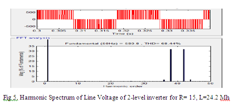
The simulation of the inverters namely conventional three and two level inverter was carried using sinusoidal pulse width modulation (SPWM) .it has shown that decrease in voltage and current THD in moving from two level inverter to three level inverter. This paper briefly explains theory of sinusoidal pulse width modulation (SPWM) for two and three level inverter and performance of both inverters was tested using RL load. It has shown that load current for three level inverter are much more sinusoidal and improvement in the line current waveform and decrease in the THD from two level to three level inverter and decrease in the THD as the frequency is increased.

REFERENCES:
[1] J. S. Lai and F.Z. Peng “Multilevel Converters – A new breed of power converters” IEEE Trans. Ind Applicant , Vol. 32, May/June 1996.
[2] Jose Roderiguez, Jih-Sheng Lai and Fang Zheng Reng, “Multilevel Inverters” A survey of topologies ,control, and applications “,IEEE Trans. On Ind.Electronics, vol No.[4], August 2002.
[3] A. Nabae, I Takashashi, and H. Akagi, “ A new neutral –point clamped PWM inverter,” IEEE Trans. Ind Application Vol. No. IA-17,PP 518-523,Sept/oc 1981.
[4] P.K.Chaturvedi, S. Jain, Pramod Agrawal “ Modeling , Simulation and Analysis of Three level Neutral Point CLAMPED inverter using matlab/Simulink/Power System Blockst”
[5] Bor-Ren Lin & Hsin – Hung Lu “ A Novel Multilevel PWM Control Scheme of the AC/DC/AC converter for AC Drives”IEEE Trans on ISIE, 1999.