asokatechnologies@gmail.com 09347143789/09949240245

Search This Blog

Friday, 27 April 2018

Development and Comparison of an Improved Incremental Conductance Algorithm for Tracking the MPP of a Solar PV Panel


ABSTRACT:
This paper proposes an adaptive and optimal control strategy for a solar photovoltaic (PV) system. The control strategy ensures that the solar PV panel is always perpendicular to sunlight and simultaneously operated at its maximum power point (MPP) for continuously harvesting maximum power. The proposed control strategy is the control combination between the solar tracker (ST) and MPP tracker that can greatly improve the generated electricity from solar PV systems. Regarding the ST system, the paper presents two drive approaches including open- and closed-loop drives. Additionally, the paper also proposes an improved incremental conductance algorithm for enhancing the speed of the MPP tracking of a solar PV panel under various atmospheric conditions as well as guaranteeing that the operating point always moves toward the MPP using this proposed algorithm. The simulation and experimental results obtained validate the effectiveness of the proposal under various atmospheric conditions.
KEYWORDS:
1.      Maximum power point tracker (MPPT)
2.       Solar tracker (ST)
3.       Solar PV panel

SOFTWARE: MATLAB/SIMULINK

 BLOCK DIAGRAM:


Fig. 1. Block diagram of the experimental setup.
EXPECTED SIMULATION RESULTS:


Fig. 2. Description of the variations of the solar irradiation and temperature.


Fig. 3. Obtained maximum output power with the P&O and improved InC algorithms under the variation of the solar irradiation.

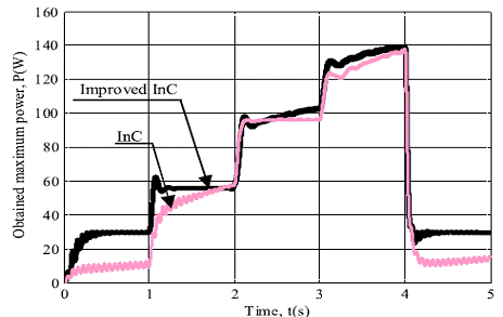
Fig. 4. Obtained maximum output power with the InC and improved InC algorithms under the variation of the solar irradiation.


Fig. 5. Obtained maximum output power with the P&O and improved InC algorithms under both the variations of the solar irradiation and temperature.

Fig. 6. Obtained maximum output power with the InC and improved InC algorithms under both the variations of the solar irradiation and temperature.


Fig. 7. MPPs of the solar PV panel under the variation of the solar irradiation


Fig. 8. MPPs of the solar PV panel under both the variations of the solar irradiation and temperature.


Fig. 9. Experimental result of obtained maximum output power with the improved InC algorithm under the variation of the solar irradiation.

CONCLUSION:
It is obvious that the adaptive and optimal control strategy plays an important role in the development of solar PV systems. This strategy is based on the combination between the ST and MPPT in order to ensure that the solar PV panel is capable of harnessing the maximum solar energy following the sun’s trajectory from dawn until dusk and is always operated at the MPPs with the improved InC algorithm. The proposed InC algorithm improves the conventional InC algorithm with an approximation which reduces the computational burden as well as the application of the CV algorithm to limit the search space and increase the convergence speed of the InC algorithm. This improvement overcomes the existing drawbacks of the InC algorithm. The simulation and experimental results confirm the validity of the proposed adaptive and optimal control strategy in the solar PV panel through the comparisons with other strategies.
REFERENCES:
[1] R. Faranda and S. Leva, “Energy comparison of MPPT techniques for PV systems,” WSES Trans. Power Syst., vol. 3, no. 6, pp. 446–455, 2008.
[2] X. Jun-Ming, J. Ling-Yun, Z. Hai-Ming, and Z. Rui, “Design of track control system in PV,” in Proc. IEEE Int. Conf. Softw. Eng. Service Sci., 2010, pp. 547–550.
[3] Z. Bao-Jian, G. Guo-Hong, and Z. Yan-Li, “Designment of automatic tracking system of solar energy system,” in Proc. 2nd Int. Conf. Ind. Mechatronics Autom., 2010, pp. 689–691.
[4] W. Luo, “A solar panels automatic tracking system based on OMRON PLC,” in Proc. 7th Asian Control Conf., 2009, pp. 1611–1614.
[5] W. Chun-Sheng,W. Yi-Bo, L. Si-Yang, P. Yan-Chang, and X. Hong-Hua, “Study on automatic sun-tracking technology in PV generation,” in Proc. 3rd Int. Conf. Elect. Utility Deregulation Restruct. Power Technol., 2008, pp. 2586–2591.

Novel Cascaded Switched-Diode Multilevel Inverter for Renewable Energy Integration


ABSTRACT:
In this paper, a new topology of two-stage cascaded switched-diode (CSD) multilevel inverter is proposed for medium voltage renewable energy integration. First, it aims to reduce the number of switches along with its gate drivers. Thus, the installation space and cost of a multilevel inverter are reduced. The spike removal switch added in the first stage of the inverter provides a flowing path for the reverse load current, and as a result, high voltage spikes occurring at the base of the stepped output voltage based upon conventional CSD multilevel inverter topologies are removed. Moreover, to resolve the problems related to dc source fluctuations of multilevel inverter used for renewable energy integration, the clock phase-shifting (CPS) one-cycle control (OCC) is developed to control the two-stage CSD multilevel inverter. By shifting the clock pulse phase of every cascaded unit, the staircase-like output voltage waveforms are obtained and a strong suppression ability against fluctuations in dc sources is achieved. Simulation and experimental results are discussed to verify the feasibility and performances of the two-stage CSD multilevel inverter controlled by the CPS OCC method.
KEYWORDS:
1.      Novel cascaded multilevel inverter
2.      Two-stage
3.      One-cycle control

SOFTWARE: MATLAB/SIMULINK

BLOCK DIAGRAM:


Fig. 1. Renewable energy generation system with multilevel inverter.


EXPECTED SIMULATION RESULTS:


Fig. 2. The output voltage and current of the first stage converter of the 5-level
simulation prototype. (a) Output voltage ug ; (b) Output current ig .


Fig. 3. The output voltage and inductor current of the 5-level simulation
prototype. (a) Output voltage uCD ; (b) Output voltage after filter uo ; (c) Inductor current il


Fig. 4. The output voltage and current of the first stage converter of the
9-level simulation prototype. (a) Output voltage ug ; (b) Output current ig .


Fig. 5. The output voltage and inductor current of the 9-level simulation
prototype. (a) Output voltage uCD ; (b) Output voltage after filter uo ; (c) Inductor current il .


Fig. 6. The simulation results of the 5-level prototype: DC source with basic
unit 1 contains a 10 Hz ripple with amplitude 16 V. (a) uo using CPS OCC; (b) uo using CPS SPWM.


Fig. 7. The simulation results of the 5-level prototype: DC source with each
basic unit contains a 10 Hz ripple with amplitude 8 V. (a) uo using CPS OCC; (b) uo using CPS SPWM.

CONCLUSION:
A new topology of two-stage CSD multilevel inverter has been proposed in this paper. n cascaded basic units and one spike removal switch form the first stage. Then by adding a full-bridge inverter as the second-stage converter, both of the positive and negative output voltage levels are generated. Since the one full-bridge converter in the output side leads to the restriction on high-voltage applications, the proposed topology is suitable for medium-voltage renewable energy integration. The comparisons with the CHB and cascaded half-bridge topologies show that the CSD topology requires less switches and related gate drivers for realizing Nlevel output voltage. As a result, the installation space and cost of the multilevel inverter are reduced. Meanwhile, the spike removal switch added in the first stage provides a flowing path for the reverse load current under R-L loads, thus, the high voltage spikes, due to the collapsing magnetic field in a very short time interval, are removed. The CPS OCC method, which is composed by n similar but dependent OCC controllers, has been designed and implemented to control the CSD multilevel inverter. Simulation and experimental results demonstrate that, by shifting the clock pulse phase of each cascaded unit, the staircase-like voltage waveforms are obtained. Moreover, to evaluate the performance of CPS OCC, in both the simulation and experiment, the DC sources mixed with low frequency ripples are implemented to simulate the DC supply from renewable energy generations, and the comparative results between CPS OCC and CPS SPWM reveal that CPS OCC possesses a superior ability in suppressing the unbalance or low frequency ripples in DC sources. These results demonstrate that the CPS OCC method can be a substitute for conventional controllers to control multilevel inverters for renewable energy integration with improved control performances.
 REFERENCES:
[1] M. S. B. Ranjiana, P. S. Wankhade, and N. D. Gondhalekar, “A modified cascaded H-bridge multilevel inverter for solar applications,” in Proc. 2014 Int. Conf. Green Comput. Commun. Elect. Eng., 2014, pp. 1–7.
[2] F. S. Kang, S. J. Park, S. E. Cho, C. U. Kim, and T. Ise, “Mutilevel PWM inverters suitable for the use of stand-alone photovoltaic power systems,” IEEE Trans. Energy Convers., vol. 20, no. 4, pp. 906–915, Dec. 2005.
[3] L. V. Nguyen, H.-D. Tran, and T. T. Johnson, “Virtual prototyping for distributed control of a fault-tolerant modular multilevel inverter for photovoltaics,” IEEE Trans. Energy Convers., vol. 29, no. 4, pp. 841–850, Dec. 2014.
[4] J. Rodriguez, J. S. Lai, and F. Z. Peng, “Mutilevel inverters: A survey of topologies, controls, and application,” IEEE Trans. Ind. Electron., vol. 49, no. 4, pp. 724–738, Aug. 2002.
[5] F. Z. Peng and J. S. Lai, “Mutilevel converters—A new breed of power converters,” IEEE Trans. Ind. Appl., vol. 32, no. 3, pp. 509–517, May/Jun. 1996.

A Single DC Source Cascaded Seven-Level Inverter Integrating Switched Capacitor Techn


 ABSTRACT:
 In this paper, a novel cascaded seven-level inverter topology with a single input source integrating switched capacitor techniques is presented. Compared with the traditional cascade multilevel inverter (CMI), the proposed topology replaces all the separate dc sources with capacitors, leaving only one H-bridge cell with a real dc voltage source and only adds two charging switches. The capacitor charging circuit contains only power switches, so that the capacitor charging time is independent of the load. The capacitor voltage can be controlled at a desired level without complex voltage control algorithm and only use the most common carrier phase-shifted sinusoidal pulse width modulation (CPS-SPWM) strategy. The operation principle and the charging-discharging characteristic analysis are discussed in detail. A 1kW experimental prototype is built and tested to verify the feasibility and effectiveness of the proposed topology.
KEYWORDS:
1.      Cascaded seven-level inverter
2.       Switched capacitor techniques
3.       Carrier phase-shifted sinusoidal pulse width modulation
4.       Charging and discharging characteristic

SOFTWARE: MATLAB/SIMULINK

 CONTROL DIAGRAM:


Fig. 1. Topologies of the proposed inverter. (a) The novel single dc source cascaded seven-level inverter. (b) Three-input cascaded seven-level inverter for PV systems.

 EXPECTED SIMULATION RESULTS:


Fig. 2. Output voltage and current waveforms. (a) At resistive load. (b) At inductive load. (c) THD value of the output voltage


Fig. 3. Voltage waveforms of the charging-switch. (a) SC1. (b) SC3.


Fig. 4. The capacitor voltage and the charging current waveforms of capacitors C1. (a) RESR=5mΩ. (b) RESR=200mΩ.

CONCLUSION:
A novel single DC source cascaded seven-level inverter integrating switched capacitor techniques is developed in this paper. In the proposed topology, the transformerless charging circuit only contains power switches and capacitors, and the charging time is independent of the load. The operation principle and the charging-discharging characteristic analysis are investigated in depth. With the common CPS-SPWM strategy, the sinusoidal output voltage can be well obtained. Moreover, the capacitors are properly charged without complex voltage balancing control algorithm. The peak charging current and the charging loss can be reduced with appropriate circuit parameters. The proposed topology has the features of modularity, low cost and simplicity of control and makes it attractive in DC-AC power applications. A 1Kw experimental prototype verifies the feasibility of the proposed inverter. The proposed inverter is also suitable for photovoltaic-battery multi-input application with high redundancy.

REFERENCES:

[1] S. Kouro, M. Malinowski, K. Gopakumar, J. Pou, L. G. Franquelo, B. Wu, J. Rodriguez, M. A. Perez, and J. I. Leon, “Recent advances and industrial applications of multilevel converters,” IEEE Trans. Ind. Electron. , vol. 57, no. 8, pp. 2553–2580, Aug. 2010.
[2] H. Abu-Rub, J. Holtz, J. Rodriguez, and G. Baoming, “Medium-voltage multilevel converters; state of the art, challenges, and requirements in industrial applications,” IEEE Trans. Ind. Electron. , vol. 57, no. 8, pp. 2581–2596, Aug. 2010.
[3] J. Dixon, J. Pereda, C. Castillo, and S. Bosch, “Asymmetrical multilevel inverter for traction drives using only one dc supply,” IEEE Trans. Veh. Technol., vol. 59, no. 8, pp. 3736–3743, Oct. 2010.
[4] S. Lu, K. A. Corzine, and M. Ferdowsi, “A unique ultracapacitor direct integration scheme in multilevel motor drives for large vehicle propulsion,” IEEE Trans. Veh. Technol., vol. 56, no. 4, pp. 1506–1515, Jul. 2007.
[5] J. Rodriguez, S. Bernet, P. K. Steimer, and I. E. Lizama, “A survey on neutral-point-clamped inverters,” IEEE Trans. Ind. Electron. , vol. 57, no. 7, pp. 2219–2230, Jul. 2010.


Thursday, 26 April 2018

Modelling and analysis of modular multilevel converter for solar photovoltaic applications to improve power quality

ABSTRACT:
The design of control circuit for a solar fed cascaded multilevel inverter to reduce the number of semiconductor switches is presented in this study. The design includes binary, trinaryand modified multilevel connection(MMC)-based topologies suitable for varying input sources from solar photovoltaics (PV). In binary mode, 2Ns +1 − 1 output voltage levels are obtained where Ns is the number of individual inverters. This is achieved by digital logic functions which includes counters, flip-flops and logic gates. In trinary mode, 3Ns levels are achieved by corresponding look-up table. MMC intends design in both control and power circuits to provide corresponding output voltage levels by appropriate switching sequences. Hence to obtain a 15-level inverter, the conventional method requires 28 switches and in binary mode 12 switches are needed. In trinary mode with the same 12 switches, 27 levels can be obtained whereas in MMC only 7 switches are employed to achieve 15 levels. The advantage of these three designs is in the reduction of total harmonic distortion by increasing the levels. Simulations are carried out in MATLAB/Simulink and comparisons were made. All the three topologies are experimentally investigated for a 3 kWp solar PV plant and power quality indices were measured.

SOFTWARE: MATLAB/SIMULINK

 CIRCUIT DIAGRAM:


Fig.1 Single stage 15-level inverter power circuit

 EXPECTED SIMULATION RESULTS:


Fig. 2 Solar PV with partial shaded condition for a 15-level CMLI
a Variation of panel irradiance
b 15-level output voltage waveform


Fig. 3 15-level output voltage waveform achieved from three stage inverter
a 15-level output voltage waveform
b FFT analysis for three stage 15-level CMLI


Fig. 4 Output voltage waveform and its corresponding harmonic spectrum
a 27-level output voltage waveform
b FFT analysis for three stage 27-level CMLI


Fig. 5 Output voltage waveform and its corresponding harmonic spectrum
a 15-level output voltage waveform
b FFT analysis for one stage 15-level CMLI


 CONCLUSION:
The power quality improvement for a solar fed CMLI with reduced number of semiconductor switches is investigated in this paper. The required 15-level output is achieved with only 12 switches in binary mode and 7 switches in MMC mode. In addition, 27-level output is obtained with 12 switches through trinary mode. The mathematical model for solar PV is carried out which is considered as the input to the inverter stages. A detailed simulation study is carried out for various levels and comparison has been made. A 3 kWp solar PV fed CMLI is implemented for all the three topologies and harmonics analysis was made. Based on the observations, the proposed method provides the multiple advantages which include reduced THD, less cost, simple design, minimum computational complexity and the absence of transformers, boost converters, detailed look-up table and filter circuit. Moreover, these methods are much suitable for standalone/grid interacted PV systems to improve power quality.
REFERENCES:
1 Rahim, N.A., Selvaraj, J.: Multistring five-level inverter with novel PWM control scheme for PV application, IEEE Trans. Ind. Electron., 2010, 57, (6), pp. 21112123
2 Selvaraj, J., Rahim, N.A.: Multilevel inverter for grid-connected PV system employing digital PI controller, IEEE Trans. Ind. Electron., 2009, 56, (1), pp. 149158
3 Rahim, N.A., Chaniago, K., Selvaraj, J.: Single-phase seven-level grid-connected inverter for photovoltaic system, IEEE Trans. Ind. Electron., 2011, 58, (6), pp. 24352443
4 Barbosa, P.G., Braga, H.A.C., do Carmo Barbosa Rodrigues, M., Teixeira, E.C.: Boost current multilevel inverter and its application on single-phase grid-connected photovoltaic systems, IEEE Trans. Power Electron., 2006, 21, (4), pp. 11161124
5 Villanueva, E., Correa, P., Rodríguez, J., Pacas, M.: Control of a single-phase cascaded H-bridge multilevel inverter for grid-connected photovoltaic systems, IEEE Trans. Ind. Electron., 2009, 56, (11), pp. 43994406