asokatechnologies@gmail.com 09347143789/09949240245

Search This Blog

Thursday, 1 November 2018

A Grid Connected Single Phase Transformerless Inverter Controlling Two Solar PV Array Operating under Different Atmospheric Conditions


ABSTRACT:
A grid connected single phase transformerless inverter which can operate two serially connected solar photo voltaic (PV) subarrays at their respective maximum power points while each one of them is exposed to different atmospheric conditions is proposed in this paper. As two subarrays are connected in series, the number of serially connected modules within a subarray is reduced to half. Reduction in the number of serially connected PV modules within a subarray leads to an overall improvement in the magnitude of power that can be abstracted from a subarray while the modules of the subarray are exposed to varied atmospheric conditions. The topological structure of the inverter ensures that the common mode voltage does not contain high frequency components, thereby reducing the magnitude of leakage current involved with the solar panels well within the acceptable limit. An in depth analysis of the scheme along with the derivation of its small signal model has been carried out. Detailed simulation studies are performed to verify its effectiveness. A 1 kW laboratory prototype of the scheme has been fabricated. Detailed experimental validations have been carried out utilizing the prototype to confirm the viability of the proposed scheme.
KEYWORDS:
1.      Grid connected single phase transformerless PV inverter
2.      Maximum power extraction
3.      Mismatched operating condition
4.      Serially connected PV subarrays

SOFTWARE: MATLAB/SIMULINK

 PROPOSED CIRCUIT DIAGRAM:


Fig. 1. Combined Half Bridge Inverter with AC Bypass (CHBIAB)

 EXPECTED SIMULATION RESULTS:


Fig.2. Simulated performance: (a) Power output from PV1 and PV2, (b) Voltage output of PV1 and PV2, (c) Output current of PV1 and PV2

Fig. 3. Simulated performance: Grid current and voltage along with their
magnified versions 

Fig. 4. Simulated performance: Output capacitor voltages along with their magnified versions

CONCLUSION:
A grid connected single phase transformerless inverter which can extract maximum power from two subarrays during  mismatched operating condition is presented in this paper. Salient features of the proposed inverter are as follows: i) number of series connected modules is less thereby reducing the effect of shading, ii) two subarrays can be operated at MPP simultaneously, thus it is well suited for PV subarrays operating under mismatched operating condition, iii) decoupled control structure is employed to control the two component half bridges of the inverter, iv) _euro of 96% is achieved which is the highest compared to the topologies dealing with solar PVs experiencing mismatched operating conditions, v) the scheme is realized through single stage of power conversion leading to a considerable reduction in size, weight and volume, vi) simple MPPT algorithm is employed thereby reducing the computational burden of the digital signal processor involved, vii) PV leakage current is limited within the limit specified in the standard, VDE 0126-1-1. The operating principle of the proposed scheme is explained in detail by exploring all the equivalent topological stages. Subsequently the mathematical analysis of the scheme has been carried out and the small signal model of the scheme has been derived. The philosophy of control is described in detail and the configuration of the controller is derived. The design guidelines for selecting the filter components of the inverter are presented. Detailed simulation and experimental studies are carried out to confirm the viability of the proposed scheme.

REFERENCES:
[1] T. Kerekes, R. Teodorescu, P. Rodriguez, G. Vazquez, and E. Aldabas, “A new high-efficiency single-phase transformerless PV inverter topology,” IEEE Trans. Industrial Electronics, vol. 58, no. 1, pp. 184-191, Jan. 2011.
[2] S. V. Araujo, P. Zacharias, and R. Mallwitz, “Highly efficient single phase transformerless inverters for grid-connected photovoltaic systems,” IEEE Trans. Industrial Electronics, vol. 57, no. 9, pp. 3118- 3128, Sep. 2010.
[3] G. M. Masters, Renewable and efficient electric power systems, New Jersey: John Wiley & Sons Inc, 2004, ISBN: 0-471-28060-7.
[4] T. Shimizu, O. Hashimoto, and G. Kimura, “A novel high-performance utility-interactive photovoltaic inverter system,” IEEE Trans. Power Electronics, vol. 18, no. 2, pp. 704-711, Mar. 2003.
[5] T. Shimizu, M. Hirakata, T. Kamezawa, and H. Watanabe, “Generation control circuit for photovoltaic modules,” IEEE Trans. Power Electronics vol. 16, no. 3, pp. 293-300, May 2001.

Wednesday, 31 October 2018

A New Design Method of an LCL Filter Applied in Active DC-Traction Substations


ABSTRACT:
This paper concentrates on the LCL filter with damping resistance intended to connect the shunt active power filter of an active DC-traction substation to the point of common coupling with the transmission grid. In order to find design conditions and conceive a design algorithm, attention is directed to the transfer functions related to currents and the associated frequency response. The mathematical foundation of the design method is based on the meeting the requirements related to the significant attenuation of the high-frequency switching current, concurrently with the unalterated flow of the current that needs to be compensated by active filtering. It is pointed out that there are practical limitations and a compromise must be made between the two requirements. To quantify the extent to which the harmonics to be compensated are influenced by imposing the magnitude response at both highest harmonic frequency to be compensated and switching frequency, a performance indicator is defined. As an additional design criterion, the damping power losses are taken into consideration. The validity and effectiveness of the proposed method are proved by simulation results and experimental tests on a laboratory test bench of small scale reproducing the specific conditions of a DC-traction substation with six-pulse diode rectifier.
KEYWORDS:
1.      DC-traction substations
2.      LCL filter
3.      Passive damping
4.      Regeneration
5.      Shunt active power filters

SOFTWARE: MATLAB/SIMULINK
BLOCK DIAGRAM:


Fig. 1. Block diagram of the active DC-traction substation.
EXPECTED SIMULATION RESULTS:


Fig. 2. Voltages and currents in the TT’s primary in traction regime


Fig. 3. LCL filter input current.


 Fig. 4. Current flowing through the capacitor of the interface filter.


Fig. 5. Harmonic spectra of the LCL filter input current (black bars) and output current (yellow bars) for harmonic order k[1, 37].


Fig. 6. Voltages and currents upstream of PCC during the operation in traction regime.

Fig. 7. Succesive traction (filtering) and braking (regeneration) regimes: (a)
phase voltage (blue line) and supply current (green line); (b) DC-capacitor
voltage (black line) and DC-line voltage (red line).


CONCLUSION:
A new design method of an LCL filter with damping resistance intended to couple the three-phase VSI of an active DC-traction substation to the power supply has been proposed in this paper. The following elements of originality are outlined.
1) The theoretical substantiation is based on the frequency response from transfer functions related to currents, taking into account the existence of the series damping resistances.
2) The expressed amplitude response and resonance frequency highlight their dependence on only pairs L2Cf and RdCf, It is a very important finding for the conceived design algorithm.
3) The expression of the power losses in the damping resistances is highlighted and an equivalent resistance is introduced as a quantitative indicator of them.
4) By considering the switching frequency as main parameter and taking into consideration the frequency of the highest order harmonic to be compensated, the design algorithm is based on the imposition of the associated attenuations.
5) In the substantiation of the design algorithm, a detailed analysis is performed on the existence of physical-sense solutions, providing the domain in which the values of the parameters must be located.
6) As a large number of parameters values sets can be obtained, a new performance indicator (MPI) is proposed, to quantify the extent to which the harmonics to be compensated are influenced.
The analysis and the simulation results achieved for an active DC-traction substation with six-pulse diode rectifier and LCL coupling filter have indicated that the proposed method is valid and effective. The experimental tests conducted in a laboratory test bench of small scale reproducing the specific conditions of a DC-traction substation illustrate good performance of the system for active filtering and regeneration connected to the power supply by the passive damped LCL filter.
The design proposal can be applied in any three-phase LCL-filter-based shunt active power filter.
REFERENCES:
[1] A. Ghoshal and V. John, “Active damping of LCL filter at low switching to resonance frequency ratio,” IET Power Electron., vol. 8, no. 4, pp. 574–582, 2015.
[2] G. E. Mejia Ruiz, N. Munoz, and J. B. Cano, “Modeling, analysis and design procedure of LCL filter for grid connected converters,” in Proc. 2015 IEEE Workshop Power Electron. and Power Quality Appl.  (PEPQA), pp. 1–6.
[3] M. Hanif, V. Khadkikar, W. Xiao, and J. L. Kirtley, “Two degrees of freedom active damping technique for filter-based grid connected PV systems,” IEEE Trans. Ind. Electron., vol. 61, no. 6, pp. 2795–2803, June 2014.
[4] X. Wang, F. Blaabjerg, and P. C. Loh, “Grid-current-feedback active damping for LCL resonance in grid-connected voltage source converters,” IEEE Trans. Power Electron., vol. 31, pp. 213–223, 2016.
[5] W. Xia, J. Kang, “Stability of LCL-filtered grid-connected inverters with capacitor current feedback active damping considering controller time delays,” J. Mod. Power Syst. Clean Energy, vol. 5, no. 4, pp. 584– 598, July 2017.

An Improved Modulated Carrier Control with On-Time Doubler for Single-Phase Shunt Activ


 ABSTRACT:
This paper proposes an improved modulated carrier control with on-time doubler for the single-phase shunt active power filter, which eliminates harmonic and reactive currents drawn by nonlinear loads. This control method directly shapes the line current to be sinusoidal and in phase with the grid voltage by generating a modulated carrier signal with a resettable integrator, comparing the carrier signal to the average line current and making duty ratio doubled. Since the line current compared to the carrier signal is not the peak, but the average value, dc-offset appeared at the conventional control methods based on one-cycle control is effectively addressed. The proposed control technique extirpates the harmonic and reactive currents and solves the dc-offset problem. The operation principle and stability characteristic of the single-phase shunt active power filter with the proposed control method are discussed, and experimental results with laboratory prototype under various load conditions verify its performance.
KEYWORDS:

1.      Single-phase shunt active power filter
2.       Modulated carrier control
3.       Indirect control
4.      One-cycle control
5.      Harmonic and reactive currents elimination
6.      Nonlinear load

SOFTWARE: MATLAB/SIMULINK

CIRCUIT DIAGRAM:


Fig. 1. Single-phase shunt active power filter with nonlinear load.
.
EXPECTED SIMULATION RESULTS


Fig. 2. Measured grid voltage, line current, APF current and load current waveforms of the shunt APF system based on the proposed control method at full load condition (vin : 200 V/div, iin : 20 A/div, if : 20 A/div, i- L : 20 A/div).


Fig. 3. Measured grid voltage, line current, APF current and load current waveforms of the shunt APF system based on the proposed control method at half load condition (vin : 200 V/div, iin : 20 A/div, if : 20 A/div, iL : 20 A/div).

Fig. 4. Current controller swithcing mechanism.


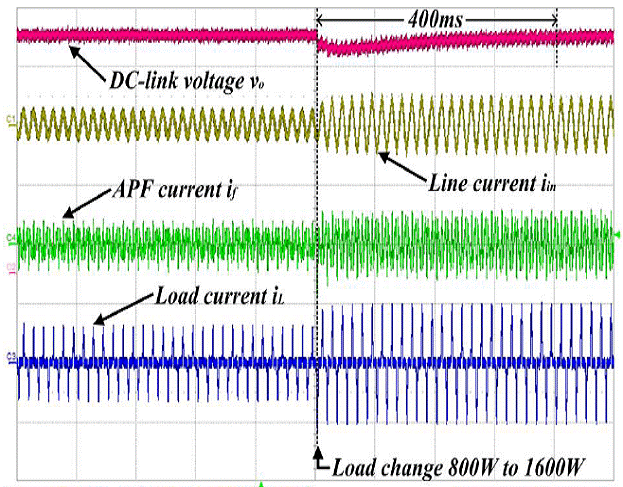
 Fig. 5. Measured dc-link voltage, line current, APF current and load current waveforms of the shunt APF system in load transient from 800 W to 1600 W (vo : 100 V/div, iin : 20 A/div, if : 20 A/div, iL : 20 A/div).

Fig. 6. Measured grid voltage, line current, APF current and load current waveforms of the shunt APF system at 110 Vrms grid voltage. (vin : 100 V/div, iin : 10 A/div, if : 10 A/div, iL : 10 A/div) Under (a) 200 W, (b) 270 W, (c) 340 W, (d) 400 W load condition.

CONCLUSION:
An improved modulated carrier control for single-phase active power filter has been proposed. The shunt APF with the proposed control method fulfills harmonic and reactive current elimination at the line current by comparing the carrier signal to the average line current and having the duty ratio doubled. On top of that, the control method totally gets rid of the dc-offset problem arisen at the conventional one based on one-cycle control and ameliorates the current control loop stability without additional ramp signal. The operation principle of power stage, the main control mechanism, and the stability characteristic of the current control loop are analyzed in detail. Experimental results with the shunt APF system under assorted conditions verify the performance of the proposed control method in steady and transient states.
REFERENCES:
[1] Elham B. Makram, E.V. Subramaniam, Adly A. Girgis, and Ray Catoe, “Hamonic filter design using actual recorded data,” IEEE Transaction on Industrial Application, vol. 29, no. 6, pp. 1176-1183, Nov. 1993.
[2] F. Z. Peng, “Harmonic sources and filtering approaches,” IEEE Transaction on Industrial Application Magazine, vol. 7, no. 4, pp. 18-25, Jul. /Aug. 2001.
[3] Czarnecki, L. S., Ginn, H. L., “The effect of the design method on efficiency of resonant harmonic filters,” IEEE Transactions on Power Delivery, vol. 20, no. 1, pp. 286-291, Jan. 2005.
[4] Fakhralden A. Huliehel, Fred C. Lee, and Bo H. Cho, “Small-signal modeling of the single-phase boost high power factor converter with constant frequency control,” PESC’92 Record. 23rd annual IEEE Power electronics Specialists Conference, 1992, vol.1, pp. 475 – 482.
[5] R. Martinez, P. N. Enjeti, “A higj-performance single-phase rectifier with input power factor correction,” IEEE Transactions on Power Electronics, vol. 11, no. 2, pp. 311–317, Mar. 1996.


A Bridge Modular Switched-Capacitor-Based Multilevel Inverter With Optimized SPWM Control Method And Enhanced Power-Decoupling Ability


ABSTRACT:
Micro-inverters operating into the single-phase grid from new energy source with low-voltage output face the challenges of efficiency bottleneck and twice-line-frequency variation. This paper proposed a multilevel inverter based on bridge modular switched-capacitor (BMSC) circuits with its superiority in conversion efficiency and power density. The topology is composed of DC-DC and DC-AC stages with independent control for each stage, aiming to improve system stability and simplify the control method. The BMSC DC-DC stage, which can be expanded to synthesize more levels, not only features multilevel voltage gain but also partially replaces the original bulk input capacitor and functions as an active energy buffer to enhance power decoupling ability between DC and AC sides. In DC-AC stage, the control strategy of optimized unipolar frequency doubling sine-wave pulse-width modulation (UFD-SPWM) is proposed to  improve the quality of output waveform. Meanwhile, the multilevel voltage phase has been optimized to reduce the power loss further. Finally, a prototype has been built and tested. Associated with the simulation, the experimental results validate the practicability of these analyses.
KEYWORDS:
1.      Switched-capacitor circuit
2.      Multilevel inverter
3.      Power decoupling
4.      Optimized unipolar frequency doubling SPWM.

SOFTWARE: MATLAB/SIMULINK

CIRCUIT DIAGRAM:


(a)

(b)
Fig.1 Topology of the proposed converter.(a) General topology of bridge  modular switched-capacitor-based multilevel inverter (b) Seven-level inverter.

EXPECTED SIMULATION RESULTS


(a)


(b)

 (c)


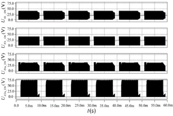
Fig.2 Simulation waveforms of seven-level inverter.(a) Us1_DS, Us3_DS, Us1a_DS
and Us2a_DS. (b) UC2a, Ud, UX, Uo and io. (c) Spectrum of Uo.


(a)


 (b)


(c)


(d)
Fig.3 Simulation comparison of power decoupling ability at different Cin. Under proposed control strategy:(a)Ui and Po. (b)Ud and Po. Under conventional control strategy:(c) Ui and Po. (d) Ud and Po.

CONCLUSION:
A bridge modular switched-capacitor-based multilevel inverter with optimized UFD-SPWM control method is proposed in the paper. The switched-capacitor-based stage can obtain high conversion efficiency and multiple voltage levels. Meanwhile, it functions as an active energy buffer, enhancing the power decoupling ability and conducing to cut the total size of the twice-line energy buffering capacitance. Furthermore, voltage multi-level in DC-link reduces the switching loss of inversion stage because turn-off voltage stress of switches changes with phase of output voltage rather than always suffers from one relatively high DC voltage. Most importantly, the control method of UFD-SPWM, doubling equivalent witching frequency, is employed in the inversion stage for a high quality output waveform with reduced harmonic. In addition, the optimized voltage level phase maximizes the fundamental component in output voltage pulses to reduce harmonic backflow as possible. Hence, the comprehensive system efficiency has been promoted and up to peak value of 97.6%. Finally, two conversion stages are controlled independently for promoting reliability and decreasing complexity. In future work, detailed loss discussion, including theoretic calculation and validation of loss breakdown, will be presented.

REFERENCES:
[1] M. Jun, "A new selective loop bias mapping phase disposition PWM with dynamic voltage balance capability for modular multilevel converter," IEEE Trans. Ind. Electron., vol. 61, no. 2, pp. 798-807, Feb. 2014.
[2] N. Mehdi, and G. Moschopoulos, "A novel single-stage multilevel type full-bridge converter," IEEE Trans. Ind. Electron., vol. 60, no. 1, pp. 31-42, Jan. 2013.
[3] E. Ehsan and N. B. Mariun, "Experimental results of 47-level switchladder multilevel inverter," IEEE Trans. Ind. Electron., vol. 60, no. 11, pp. 4960-4967, Nov. 2013.
[4] J. Lai, “Power conditioning circuit topologies,” IEEE Trans. Ind. Electron., vol. 3, no. 2, pp. 24-34, Jun. 2009.
[5] L. He, C. Cheng, “Flying-Capacitor-Clamped Five-Level Inverter Based on Switched-Capacitor Topology,” IEEE Trans. Ind. Electron., vol. 63, no.12, pp. 7814-7822, Sep. 2016.