asokatechnologies@gmail.com 09347143789/09949240245

Search This Blog

Tuesday, 22 February 2022

A Modified Cascaded H-Bridge Multilevel Inverter For Solar Applications

 ABSTRACT:

In this paper, a modified cascaded H-bridge multilevel inverter (MLI) is proposed and designed for solar applications. Generally, as the level of conventional multilevel inverter increases, the required number of switches and size increases. The proposed topology is cascade of unit stages which involves 5 switches and two voltage source; moreover a unit stage is capable of generating 5 levels. Also, the detailed analysis of cascaded multilevel inverter is discussed which incorporates three different methodologies involving less number of power devices in order to generate maximum number of levels. This results into reduction in gate drive circuitry and less switching losses. The proposed MLI is designed for power 1.5kW and In phase level shifting SPWM technique has been incorporated in which 5kHz carrier wave is compared with 50Hz of sinusoidal wave with a modulation index of 0.8. As a result, total harmonic distortion (THD) is achieved as 4.71% with LC-filter for above mentioned multilevel inverter. The circuits are modeled and simulated with the help of MATLAB/SIMULINK.

KEYWORDS:

1.      Modified cascaded H-bridge MLI

2.      Solar

3.      SPWM techniques

4.      Total Harmonic Distortions

 SOFTWARE: MATLAB/SIMULINK

 BLOCK DIAGRAM:

Fig1. Proposed N-level modified cascaded MLI

 EXPECTED SIMULATION RESULTS:


Fig.2 Output voltage and current waveforms (9-level) without filter


Fig.3 Output voltage and current waveform (9-level) with LC- filter


Fig.4 (a)-(c) Gate Pulse for 10 switches


Fig.5 Output voltage and current waveforms (13-level) without filter


Fig.6 Output voltage and current waveform (13-level) with LC- filter


Fig.7 Output voltage and current waveforms (17-level) without filter


Fig.8 Output voltage and current waveform (17-level) with LC- filter


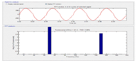
Fig.9 THD of 9-level (first methodology) without filter


Fig.10 THD of 9-level (first methodology) with filter

Fig.11 THD of 13-level (Second methodology) without filter


Fig.12 THD of 13-level (second methodology) with filter


Fig.13 THD of 17-level (Third methodology) without filter


Fig.14 THD of 17-level (Third methodology) with filter


 CONCLUSION:

 In this paper, a new topology of modified cascaded H bridge MLI is designed for solar high power application. The three different methodologies have been analyzed and 9-level, 13-level and 17-level output is observed in the respective methodology. The number of switches used in the topology is less which in turn reduced the corresponding gate driving circuitry and made the circuit compact in size. The circuits of proposed MLI are simulated in MATLAB/SIMULINK and total harmonic distortions for the three methodologies are obtained by using FFT analysis window. The lowest THD observed with LC-filter is 4.71%. The proposed MLI is designed for power 1.5kW and In-Phase level shifting method is followed for the pulse generation for all three methodologies.

REFERENCES:

[1] Wei Zhao; Hyuntae Choi; G. Konstantinou; M. Ciobotaru; and V. G. Agelidis “Cascaded H-bridge Multilevel Converter for Large-scale PV Grid-Integration with Isolated DC-DC stage” PEDG, IEEE 2012.

[2] S. Rivera; S. Kouro; B. Wu; J. I. Leon; J. Rodriguez; and L. G. Franquelo "Cascaded H-bridge multilevel converter multistring topology for large scale photovoltaic systems," IEEE ISIE 2011, pp.1837-1844.

[3] N.A. Rahim; K. Chaniago; and J. Selvaraj "Single-Phase Seven-Level Grid Connected Inverter for Photovoltaic System", IEEE Transactions on Industrial Electronics, Vol. 58, No. 6, June 2011, pp. 2435-2443

[4] B. Singh; N. Mittal; and K. S. Verma “Multi-Level Inverter: A Literature Survey On Topologies And Control Strategies”, International Journal of Reviews in Computing, Vol. 10, July 2012, pp. 1-16

[5] Zhiguo pan; F .Z Peng; Victor Stefanoic; and Mickey Leuthen “A Diode-Clamped Multilevel Converter with Reduced Number of Clamping Diodes.”2004 IEEE.


A Modified Carrier-Based Advanced Modulation Technique for Improved Switching Performance of Magnetic Linked Medium Voltage

 ABSTRACT:

 The high-frequency magnetic link is gaining popularity due to its light weight, small volume, and inherent voltage balancing capability. Those features can simplify the utilization of multilevel converter (MLC) for the integration of renewable energy sources to the grid with compact size and exert economic feasibility. The modulation and control of MLC are crucial issues especially for grid connected applications. To support the grid, the converter may need to operate in over-modulation (OVM) region for short periods depending upon the loading conditions. This OVM operation of the converter causes increased harmonic losses and adverse effects on overall system efficiency. On top of that, the size and cost of filtering circuitry become critical to eliminate the unwanted harmonics. In this regard, a modified OVM scheme with phase disposed carriers for grid connected high frequency magnetic link-based cascaded H-bridge (CHB) MLC is proposed for the suppression of harmonics and the reduction of converter loss. Furthermore, with the proposed OVM technique, the voltage gain with modulation index can be increased up to the range which is unlikely to be achieved using the classical ones. Extensive simulations are carried out with a 2.24 MVA permanent magnet synchronous generator-based wind energy conversion system which is connected to the 11 kV ac grid through a high-frequency magnetic link and a 5-level CHB MLC. A scaled down laboratory prototype is implemented to validate the performance of the converter.

KEYWORDS:

1.      Multilevel converter

2.      Over modulation

3.      Grid connection

4.      High-frequency magnetic link

5.      Wind energy

SOFTWARE: MATLAB/SIMULINK

BLOCK DIAGRAM:


Fig. 1. Control scheme for high-frequency magnetic link coupled, five-level cascaded H-bride converter-based grid-connected wind energy conversion system.

EXPECTED SIMULATION RESULTS:


Fig.2. Fundamental voltage (normalized) in OVM region: (a) regular and (b) proposed methods.


Fig. 3. Simulated performance of the system: (a) dq current components, (b) rated output power, (c) line voltage, (d) dc-link voltage, and (e) converter side line voltage.


Fig. 4. Carrier signal modification to go from linear modulation to OVM mode (frequency is deliberately reduced to have better view).

Fig. 5. Simulated performance of the system after load inclusion for sinusoidal PWM: (a) dq current components, (b) output reference signals from the controller, (c) line voltage (after filter), (d) line current (after filter), and (e) dc-link voltage.


Fig. 6. Converter output voltage profiles with momentary OVM region for different modulation schemes: (a) SPWM, (b) THSDBCPWM, (c) SSDBCPWM, and (d) THPWM.


Fig. 7. (a) High-frequency gate pulses to drive high frequency inverter and (b) gate pulse generation from DSP F28335 for single phase voltage generation of five-level CHB converter (proposed OVM with third harmonic injected signal).


Fig. 8. (a) High-frequency magnetic link primary and secondary voltage with rectified output voltage and (b) primary and secondary voltage with corresponding magnetizing current.


Fig. 9. (a) B-H loop of the core with high-frequency excitation with 1.2 μs dead-band and (b) core loss with 10 kHz square wave excitation.


Fig. 10. Converter overall performance under existing (left column) and proposed (right column) OVM technique with third harmonic injected signal.

CONCLUSION:

To improve the system performance, a modified OVM technique is presented in this paper with grid connected and islanded operation. With the proposed modified carrier signal based BCPWM techniques, the overall loss and THD are decreased for both the islanded and grid connected modes compared with the traditional OVM techniques. Moreover, the voltage gain can be increased and remains approximately constant in the proposed method, which may not be possible to obtain using the traditional OVM methods. In this paper, a high-frequency magnetic link-based fully-rated CHB converter is developed for wind energy applications and the behavior of the system under rated and overrated load conditions are investigated.The use of magnetic link for the generation of isolated and balanced dc sources of the MLC inherently overcomes the voltage imbalance problem of CHB MLC and hence effectively simplifies the system control complexities. The core loss of high-frequency magnetic link is also measured to identify the overall loss of the system. The effectiveness of the proposed technology is confirmed by the simulation and experimental results.


REFERENCES:

[1] M. R. Islam, Y. G. Guo, J. G. Zhu, H. Lu, and J. X. Jin, “High-frequency magnetic-link medium-voltage converter for superconducting generator-based high-power density wind generation systems,” IEEE Trans. Appl. Supercond., vol. 24, no. 5, pp. 1–5, Oct. 2014.

[2] N. Mendis, K. M. Muttaqi, S. Perera, and S. Kamalasadan, “An effective power management strategy for a wind–diesel–hydrogen-based remote area power Supply System to meet fluctuating demands under generation uncertainty,” IEEE Trans. Ind. Appl., vol. 51, no. 2, pp. 1228–1238, Mar.–Apr. 2015.

[3] B. Jain, S. Jain, and R. K. Nema, “Control strategies of grid interfaced wind energy conversion system: An overview,” Renew. Sustain. Energy Rev., vol. 47, pp. 983–996, Apr. 2015.

[4] Y. Tan, K. M. Muttaqi, P. Ciufo, and L. Meegahapola, “Enhanced frequency response strategy for a PMSG-based wind energy conversion system using ultracapacitor in remote area power supply systems,” IEEE Trans. Ind. Appl., vol. 53, no. 1, pp. 549–558, Jan.–Feb. 2017.

[5] M. R. Islam, Y. G. Guo, and J. G. Zhu, “A multilevel medium-voltage inverter for step-up-transformer-less grid connection of photovoltaic power plants,” IEEE J. Photovolt., vol. 4, no. 3, pp. 881‒889, May 2014.


A Highly Efficient and Reliable Inverter Configuration Based Cascaded Multi-Level Inverter for PV Systems

 ABSTRACT:

This paper presents an improved Cascaded Multi-Level Inverter (CMLI) based on a highly efficient and reliable configuration for the minimization of the leakage current. Apart from a reduced switch count, the proposed scheme has additional features of low switching and conduction losses. The proposed topology with the given PWM technique reduces the high-frequency voltage transitions in the terminal and common-mode voltages. Avoiding high-frequency voltage transitions achieves the minimization of the leakage current and reduction in the size of EMI filters. Furthermore, the extension of the proposed CMLI along with the PWM technique for 2m+1 levels is also presented, where m represents the number of Photo Voltaic (PV) sources. The proposed PWM technique requires only a single carrier wave for all 2m+1 levels of operation. The Total Harmonic Distortion (THD) of the grid current for the proposed CMLI meets the requirements of IEEE 1547 standard. A comparison of the proposed CMLI with the existing PV Multi-Level Inverter (MLI) topologies is also presented in the paper. Complete details of the analysis of PV terminal and common-mode voltages of the proposed CMLI using switching function concept, simulations, and experimental results are presented in the paper.

KEYWORDS:

1.      Cascaded multi-level inverter

2.      Leakage current

3.      Common-mode voltage

4.      Terminal voltage

SOFTWARE: MATLAB/SIMULINK

BLOCK DIAGRAM:


Fig. 1. Proposed five-level grid-connected CMLI with PV and parasitic elements.

 EXPECTED SIMULATION RESULTS:

Fig. 2. Simulation results of proposed five-level CMLI showing the waveforms of : (a) output voltage vuv; (b) grid current iac; (c) terminal voltage vxg; (d) terminal voltage vyg; (e) terminal voltage vzg; (f) leakage current ileak; (g) common-mode voltage vcm.

CONCLUSION:


In this paper, an improved five-level CMLI with low switch count for the minimization of leakage current in a transformerless PV system is proposed. The proposed CMLI minimizes the leakage current by eliminating the high-frequency transitions in the terminal and common-mode voltages. The proposed topology also has reduced conduction and switching losses which makes it possible to operate the CMLI at high switching frequency. Furthermore, the solution for generalized 2m+1 levels CMLI is also presented in the paper. The given PWM technique requires only one carrier wave for the generation of 2m+1 levels. The operation, analysis of terminal and common-mode voltages for the CMLI is also presented in the paper. The simulation and experimental results validate the analysis carried out in this paper. The MPPT algorithm is also integrated with the proposed five-level CMLI to extract the maximum power from the PV panels. The proposed CMLI is also compared with the other existing MLI topologies in Table V to show its advantages.

REFERENCES:

[1] Y. Tang, W. Yao, P.C. Loh and F. Blaabjerg, "Highly Reliable Transformerless Photovoltaic Inverters With Leakage Current and Pulsating Power Elimination," IEEE Trans. Ind. Elect., vol. 63, no. 2, pp. 1016-1026, Feb. 2016.

[2] W. Li, Y. Gu, H. Luo, W. Cui, X. He and C. Xia, "Topology Review and Derivation Methodology of Single-Phase Transformerless Photovoltaic Inverters for Leakage Current Suppression," IEEE Trans. Ind. Elect., vol. 62, no. 7, pp. 4537-4551, July 2015.

[3] J. Ji, W. Wu, Y. He, Z. Lin, F. Blaabjerg and H. S. H. Chung, "A Simple Differential Mode EMI Suppressor for the LLCL-Filter-Based Single-Phase Grid-Tied Transformerless Inverter," IEEE Trans. Ind. Elect., vol. 62, no. 7, pp. 4141-4147, July 2015.

[4] Y. Bae and R.Y.Kim, "Suppression of Common-Mode Voltage Using a Multicentral Photovoltaic Inverter Topology With Synchronized PWM," IEEE Trans. Ind. Elect., vol. 61, no. 9, pp. 4722-4733, Sept. 2014.

[5] N. Vazquez, M. Rosas, C. Hernandez, E. Vazquez and F. J. Perez-Pinal, "A New Common-Mode Transformerless Photovoltaic Inverter," IEEE Trans. Ind. Elect., vol. 62, no. 10, pp. 6381-6391, Oct. 2015.


Friday, 11 February 2022

A Five-Level Step-up Module for Multilevel Inverters: Topology, Modulation Strategy and Implementation


ABSTRACT:

 This paper proposes a new single-phase five-level converter based on switched capacitor technique. The capacitor charging in the proposed converter is carried out in a self-balancing form which does not need closed-loop modulations or additional balancing circuits. The proposed topology is a voltage booster without using end side H-bridge for changing load voltage polarity. So, switching losses and total voltage stress of semiconductor components reduce in the proposed converter. The performing modes of the proposed topology, its modulation scheme, capacitors’ balancing analysis, capacitance and loss calculations, and also the development of the proposed converter for enhancing the quality of output voltage waveform are discussed in depth. Moreover, the comparison of the proposed structure with the other multi-level topologies shows that the proposed converter can reduce the number of semiconductor elements and the required isolated DC sources. Finally, the simulation and experimental results validate the appropriate performance of the proposed converter.

KEYWORDS:

1.      Power conversion

2.      Multilevel converter

3.      Switched capacitor technique

4.      Self-balancing

5.      Phase disposition pulse width modulation technique

SOFTWARE: MATLAB/SIMULINK

PROPOSED DIAGRAM:


Fig. 1. Circuit arrangement of the proposed converter (VLoad = Va-Vb)

 EXPECTED SIMULATION RESULTS:


Fig. 2. Simulation results, (a) output waveforms with resistive load (ZL=50Ω) (b) output waveforms with resistive-inductive load (ZL=50Ω+100mH) (c) capacitors’ voltage (d) output voltage THD

Fig. 3. The simulation results with sudden change in the load (a) first scenario (b) second scenario (c) third scenario

Fig. 4. The simulation results of the capacitors’ voltage, output voltage and current in diode–rectifier state with R–C load (R=120Ω, C=2.2mF)


Fig. 5. (a) Modules’ output voltage (b) capacitors’ voltage (c) converter’s output voltage and current with ZL=100Ω (d) converter’s output voltage and current with ZL=100Ω+200mH

CONCLUSION:


In this paper, a single phase five-level switched-capacitor converter is proposed, which is combination of a switched capacitor cell (SCC) and two half-bridge cell (HBC). The capacitors’ charging in the proposed topology is carried out in self-balancing form and the charging time is independent of the load. The main idea of the proposed configuration is to reduce the number of power devices along with boosting capability. Compared to other five-level converters, the proposed topology reduces the number of DC power supplies, semiconductor switches, diodes, size and cost of the system. Simple configuration, easy control and voltage booster are the main benefits of the proposed converter. Operational modes of proposed topology and its modulation strategy, capacitors’ charging analysis and voltage stress of the switches, capacitance and power losses calculations are presented in depth. Finally, the operation and performance of the proposed converter are verified with experiments on a 5-level prototype.

REFERENCES:


[1] L. G. Franquelo, J. Rodriguez, J. I. Leon, S. Kouro, R. Portillo, and M. A. M. Prats, "The age of multilevel converters arrives," IEEE Industrial Electronics Magazine, vol. 2, pp. 28-39, 2008.

[2] F. Gao, "An Enhanced Single Phase Step-Up Five-Level Inverter," IEEE Trans. Power Electron., vol. PP, pp. 1-1, 2016.

[3] C. H. Hsieh, T. J. Liang, S. M. Chen, and S. W. Tsai, "Design and Implementation of a Novel Multilevel DC-AC Inverter," IEEE Trans. Ind. Appl., vol. 52, pp. 2436-2443, 2016.

[4] A. Nabae, I. Takahashi, and H. Akagi, "A New Neutral-Point-Clamped PWM Inverter," IEEE Trans. Ind. Appl., vol. IA-17, pp. 518-523, 1981.

[5] T. A. Meynard and H. Foch, "Multi-Level Choppers for High Voltage Applications," EPE Journal, vol. 2, pp. 45-50, 1992.


A dual control strategy for power sharing improvement in islanded mode of AC microgrid

ABSTRACT:

Parallel operation of inverter modules is the solution to increase the reliability, efficiency, and redundancy of inverters in microgrids. Load sharing among inverters in distributed generators (DGs) is a key issue. This study investigates the feasibility of power-sharing among parallel DGs using a dual control strategy in islanded mode of a microgrid. PQ control and droop control techniques are established to control the microgrid operation. P-f and Q-E droop control is used to attain real and reactive power sharing. The frequency variation caused by load change is an issue in droop control strategy whereas the tracking error of inverter power in PQ control is also a challenge. To address these issues, two DGs are interfaced with two parallel inverters in an islanded AC microgrid. PQ control is investigated for controlling the output real and reactive power of the DGs by assigning their references. The inverter under enhanced droop control implements power reallocation to restore the frequency among the distributed generators with predefined droop characteristics. A dual control strategy is proposed for the AC microgrid under islanded operation without communication link. Simulation studies are carried out using MATLAB/SIMULINK and the results show the validity and effective power-sharing performance of the system while maintaining a stable operation when the microgrid is in islanding mode.

KEYWORDS:

1.      Microgrid

2.      Inverter parallel operation control strategy

3.      Droop control strategy

4.      Frequency restore

5.      Power sharing

SOFTWARE: MATLAB/SIMULINK


BLOCK DIAGRAM:


Fig. 1 Enhanced droop control diagram

 EXPECTED SIMULATION RESULTS:

Fig. 2 Output voltage and current waveforms at PCC under the proposed dual –control


Fig. 3 Tracking output power of PQ control inverter

Fig. 4 Active power dynamics response at PCC

Fig. 5 Reactive power dynamics response at PCC

Fig. 6 Frequency variation with and without FRS

CONCLUSION:

 This letter proposes a compact nine-level T-type packed U-cell inverter. Compared with other nine-level inverters, the proposed topology has fewer power semiconductor devices and only needs two isolated dc sources. Furthermore, the proposed PWM scheme only uses one carrier, which can reduce the design and control complexity. Since the T-type leg will generate the high frequency switching waveform, it can be replaced by SiC MOSFETs for significantly reducing switching losses. Experimental results verified the performance of the proposed multilevel topology.

REFERENCES:

 [1] K. K. Gupta, A. Ranjan, P. Bhatnagar, L. Kumar Sahu, and S. Jain, “Multilevel inverter topologies with reduced device count: A review,” IEEE Trans. Power Electron., vol. 31, no. 1, pp. 135–151, Jan. 2016.

 [2] J. Rodriguez, S. Bernet, B. Wu, J. O. Pontt, and S. Kouro, “Multilevel voltage-source-inverter topologies for industrial medium-voltage drives,” IEEE Trans. Ind. Electron., vol. 54, no. 6, pp. 2930–2945, Dec. 2007.

[3] H. Abu-Rub, J. Holtz, J. Rodriguez, and G. Baoming, “Medium-voltage multilevel inverters: State of the art, challenges, and requirements in industrial applications,” IEEE Trans. Ind. Electron., vol. 57, no. 8, pp. 2581–2596, Aug. 2010.

[4] S. Kouro, M. Malinowski, K. Gopakumar, J. Pou, L. G. Franquelo, B. Wu, J. Rodriguez, M. A. Perez, and J. I. Leon, “Recent advances and industrial applications of multilevel converters,” IEEE Trans. Ind. Electron., vol. 57, no. 8, pp. 2553–2580, Aug. 2010.

[5] P. R. Bana, K. P. Panda, R. T. Naayagi, P. Siano, and G. Panda, “Recently Developed Reduced Switch Multilevel Inverter for Renewable Energy Integration and Drives Application: Topologies, Comprehensive Analysis and Comparative Evaluation,” IEEE Access, vol. 7, pp. 54888–54909, 2019.