asokatechnologies@gmail.com 09347143789/09949240245

Search This Blog

Wednesday, 23 February 2022

A New Boost Switched-Capacitor Multilevel Converter with Reduced Circuit Devices

ABSTRACT:

 In this paper, a novel platform for the single phase switched-capacitor multilevel inverters (SCMLIs) is presented. It has several advantages over the classical topologies such as: An appropriate boosting property, higher efficiency, lower number of required dc voltage sources and other accompanying components with less complexity and lower cost. The basic structure of the proposed converter is capable of making nine-level of the output voltage under different kinds of loading conditions. Hereby, by using the same two capacitors paralleled to a single dc source, a switched-capacitor (SC) cell is made that contributes to boosting the value of the input voltage. In this case, the balanced voltage of the capacitors can be precisely provided on the basis of the series-parallel technique and the redundant switching states. Afterwards, to reach the higher number of output voltage levels, two suggested SC cells are connected to each other with a new extended configuration. Therefore, by the use of a reasonable number of required power electronic devices, and also by utilizing only two isolated dc voltage sources, which their magnitudes can be designed based on either symmetric or asymmetric types, a 17- and 49-level of the output voltage are obtained. Based on the proposed extended configuration, a new generalized version of SCMLIs is also derived. To confirm the precise performance of the proposed topologies, apart from the theoretical analysis and a complete comparison, several simulation and experimental results are also given.

KEYWORDS:

1.      Charge balancing control

2.      Multilevel inverters

3.      Reduced circuit devices

4.      Switched-capacitor cell

SOFTWARE: MATLAB/SIMULINK

BLOCK DIAGRAM:


Fig. 1. Proposed Switched-capacitor multilevel inverter (SCMLI) structure

EXPECTED SIMULATION RESULTS:


Fig. 2. The nine-level output voltage and current waveforms (a) for inductive load (experiment) (200 V/div&2 A/div) (b) for resistive load (experiment) (200 V/div& 2 A/div) (c) for inductive load (simulation) (d) for resistive load (simulation).

Fig. 3. The balanced voltage of capacitors in the experiments (50 V/div).


Fig. 4. The PIVs of the involved power switches based on the experimental result.


Fig. 5. The input current waveform under the inductive loading condition based on the experimental result (2 A/div).


Fig. 6. The output voltage and current waveforms (a) from no-load to full-load (200 V/div & 5 A/div experiment) (b) from full-load to no-load (200 V/div & 5 A/div experiment) (c) from no-load to full-load (simulation) (d) from full-load to no-load (simulation).


Fig. 7. The output and capacitors voltage waveforms within a step change of load based on experimental results.


Fig. 8. Output voltage and current waveforms of the proposed symmetric 17-level structure in the experiments (250 V/div& 5 A/div).


Fig. 9. Voltage across capacitors based on the experimental results (25 V/div) (Voltage ripple 2.5 V/div).

CONCLUSION:

 In this study, a new basic topology of SCMLIs has been proposed which offers features like boosting capability, reduction in number of circuit components, higher efficiency and lower overall cost. The basic structure of the proposed SCMLI has only one dc source integrated into a novel SC cell. In this case, by aiming the series/parallel conversion of switches and also the redundant switching states, nine-level of the output voltage with only eight gate drivers has been obtained. Afterwards, in order to achieve further number of output voltage levels, an extended structure of the proposed SCMLI based on two isolated modules of the integrated SC cells has been presented. In respect to the proposed extended SCMLI, a generalized topology based on different numbers of involved SC cells has also been introduced. Then, determination of capacitance besides a power loss analysis is developed for the basic structure of the proposed SCMLI. A comprehensive comparison with other recently presented structures has also highlighted the potential of the proposed topologies. Finally, to demonstrate the precise performance of the proposed SCMLI configurations, various types of simulation and experimental tests under different kinds of loading conditions have been given.

REFERENCES:

[1] S. B. Kjaer, J K. Pedersen, and F. Blaabjerg, “A review of single-phase grid-connected inverters for photovoltaic modules,” IEEE Trans. Ind. Electron., vol. 41, no. 5, pp. 1292–1306, Sep./Oct. 2005.

[2] M. Islam, S. Mekhilef and M. Hasan, "Single phase transformerless inverter topologies for grid-tied photovoltaic system: A review", Renew. Sustainable Energy Rev., vol. 45, pp. 69-86, 2015.

[3] R. R. Errabelli, and P. Mutschler, “Fault- tolerant voltage source inverter for permanent magnet drives,” IEEE Trans. Power Electron., vol. 27, no. 2, pp. 500-508, Feb. 2012.

[4] F. Z. Peng, “Z-source inverter,” IEEE Trans. Ind. Appl., vol. 39, no. 2, pp. 504–510, Mar./Apr. 2003.

[5] H. Fathi and H. Madadi “Enhanced-boost Z-source inverters with switched Z-impedance,” IEEE. Trans. Ind. Electron, vol. 63, no. 2, pp. 691-703, Feb. 2016.

A Multi-Cell 21-Level Hybrid Multilevel Inverter synthesizes a reduced number of components with Voltage Boosting Property

 ABSTRACT:

A multi-cell hybrid 21-Level multilevel inverter is proposed in this paper. The proposed topology includes two-unit; an H-bridge is cascaded with a modified K-type unit to generate an output voltage waveform with 21 levels based only on two unequal DC suppliers. The proposed topology's advantage lies in the fine and clear output voltage waveforms with high output efficiency. Meanwhile, the high number of output voltage waveform levels generates a low level of distortion and reduces the level of an electromagnetic interface (EMI). Moreover, it reduces the voltage stress on the switching devices and gives it a long lifetime. Also, the reduction in the number of components has a noticeable role in saving size and cost. Regarding the capacitors charging, the proposed topology presents an online method for charging and balancing the capacitor's voltage without any auxiliary circuits. The proposed topology can upgrade to a high number of output steps through the cascading connection. Undoubtedly this cascading will increase the power level to medium and high levels and reduce the harmonics content to a neglectable rate. The proposed system has been tested through the simulation results, and an experimental prototype based on the controller dSPACE (DS-1103) hardware unit used to support the simulation results.

KEYWORDS:


1.      21-Level Multilevel Inverter (MLI)

2.      Hybridization

3.      Modified K-type inverter

4.      Online charging

5.      Self-balancing

6.      Voltage boosting inverter

7.      Total Harmonic Distortion (THD)

SOFTWARE: MATLAB/SIMULINK

 BLOCK DIAGRAM:

Figure.1 Proposed Hybrid MLI Topology

 EXPECTED SIMULATION RESULTS:


Figure.2 21L MLI output voltage waveform

Figure.3 FFT analysis of the 21L output voltage waveform


Figure.4 Capacitor voltages and the output voltage waveform


Figure.5 Output voltage and load current waveforms


Figure.6 63L cascaded system output voltage and load current


Figure.7 FFT analysis of the 63L output voltage waveform


Figure.8 Output voltages of 2HB+K cascaded system units


Figure.9 147L cascaded system output voltage and load current


Figure.10 FFT analysis of the 147L output voltage waveform


Figure.11 Output voltages of Asymmetrical cascaded system units

 CONCLUSION:

 The work in this paper presented a hybrid multilevel inverter that consisted of a series connection between two units (an HB unit with a modified K-Type unit). This combination generates an output voltage waveform with 21 steps. This high number steps in the output voltage help in reducing the level of noises in the output voltage and reduced the stress in the switching devices, which on the one hand generating fine and clear waveforms and on the other hand reduces the harmonic content in the waveforms to a deficient level (satisfying the harmonics standard IEEE519). Economically, the structure of the proposed topology presented an optimal design in terms of reducing the number of switches and DC sources which in turn enhancing the system reliability by reducing the inverter cost. For the capacitors charging process, the paper presents an online method for charging and balancing the capacitor voltages without any auxiliary circuits for that. This helps in the continuous operation of the charging and discharging process for the capacitor without disturbing the process of generating the output voltage. The proposed topology supports the modularity process in order to maximize the range of output power to the medium and high level, and the paper presented two scenarios for the series connection 2HB+K and HB+2K both the cases raise the level of the output power and enhances the system performance to achieve high efficiency. Due to the dependence on multi DC sources, this topology is suitable for renewable energy applications; DC sources are abundant. The hybrid renewable energy sources application will be more appropriate between all the renewable energy applications because the proposed topology-based mainly on two unequal DC suppliers, which will be available easily in the hybrid renewable energy sources.

 REFERENCES:

[1] F. Z. Peng, W. Qian, and D. Cao, "Recent advances in multilevel converter/inverter topologies and applications," in The 2010 International Power Electronics Conference-ECCE ASIA-, 2010, pp. 492-501.

[2] J. Rodriguez, J.-S. Lai, and F. Z. Peng, "Multilevel inverters: a survey of topologies, controls, and applications," IEEE Transactions on Industrial Electronics, vol. 49, pp. 724-738, 2002.

[3] L. M. Tolbert and X. Shi, "Multilevel power converters," in Power Electronics Handbook, ed: Elsevier, 2018, pp. 385-416.

[4] K. K. Gupta, A. Ranjan, P. Bhatnagar, L. K. Sahu, and S. Jain, "Multilevel inverter topologies with reduced device count: A review," IEEE transactions on power electronics, vol. 31, pp. 135-151, 2015.

[5] P. Omer, J. Kumar, and B. S. Surjan, "A Review on Reduced Switch Count Multilevel Inverter Topologies," IEEE Access, vol. 8, pp. 22281-22302, 2020.

Tuesday, 22 February 2022

A Modified Cascaded H-Bridge Multilevel Inverter For Solar Applications

 ABSTRACT:

In this paper, a modified cascaded H-bridge multilevel inverter (MLI) is proposed and designed for solar applications. Generally, as the level of conventional multilevel inverter increases, the required number of switches and size increases. The proposed topology is cascade of unit stages which involves 5 switches and two voltage source; moreover a unit stage is capable of generating 5 levels. Also, the detailed analysis of cascaded multilevel inverter is discussed which incorporates three different methodologies involving less number of power devices in order to generate maximum number of levels. This results into reduction in gate drive circuitry and less switching losses. The proposed MLI is designed for power 1.5kW and In phase level shifting SPWM technique has been incorporated in which 5kHz carrier wave is compared with 50Hz of sinusoidal wave with a modulation index of 0.8. As a result, total harmonic distortion (THD) is achieved as 4.71% with LC-filter for above mentioned multilevel inverter. The circuits are modeled and simulated with the help of MATLAB/SIMULINK.

KEYWORDS:

1.      Modified cascaded H-bridge MLI

2.      Solar

3.      SPWM techniques

4.      Total Harmonic Distortions

 SOFTWARE: MATLAB/SIMULINK

 BLOCK DIAGRAM:

Fig1. Proposed N-level modified cascaded MLI

 EXPECTED SIMULATION RESULTS:


Fig.2 Output voltage and current waveforms (9-level) without filter


Fig.3 Output voltage and current waveform (9-level) with LC- filter


Fig.4 (a)-(c) Gate Pulse for 10 switches


Fig.5 Output voltage and current waveforms (13-level) without filter


Fig.6 Output voltage and current waveform (13-level) with LC- filter


Fig.7 Output voltage and current waveforms (17-level) without filter


Fig.8 Output voltage and current waveform (17-level) with LC- filter


Fig.9 THD of 9-level (first methodology) without filter


Fig.10 THD of 9-level (first methodology) with filter

Fig.11 THD of 13-level (Second methodology) without filter


Fig.12 THD of 13-level (second methodology) with filter


Fig.13 THD of 17-level (Third methodology) without filter


Fig.14 THD of 17-level (Third methodology) with filter


 CONCLUSION:

 In this paper, a new topology of modified cascaded H bridge MLI is designed for solar high power application. The three different methodologies have been analyzed and 9-level, 13-level and 17-level output is observed in the respective methodology. The number of switches used in the topology is less which in turn reduced the corresponding gate driving circuitry and made the circuit compact in size. The circuits of proposed MLI are simulated in MATLAB/SIMULINK and total harmonic distortions for the three methodologies are obtained by using FFT analysis window. The lowest THD observed with LC-filter is 4.71%. The proposed MLI is designed for power 1.5kW and In-Phase level shifting method is followed for the pulse generation for all three methodologies.

REFERENCES:

[1] Wei Zhao; Hyuntae Choi; G. Konstantinou; M. Ciobotaru; and V. G. Agelidis “Cascaded H-bridge Multilevel Converter for Large-scale PV Grid-Integration with Isolated DC-DC stage” PEDG, IEEE 2012.

[2] S. Rivera; S. Kouro; B. Wu; J. I. Leon; J. Rodriguez; and L. G. Franquelo "Cascaded H-bridge multilevel converter multistring topology for large scale photovoltaic systems," IEEE ISIE 2011, pp.1837-1844.

[3] N.A. Rahim; K. Chaniago; and J. Selvaraj "Single-Phase Seven-Level Grid Connected Inverter for Photovoltaic System", IEEE Transactions on Industrial Electronics, Vol. 58, No. 6, June 2011, pp. 2435-2443

[4] B. Singh; N. Mittal; and K. S. Verma “Multi-Level Inverter: A Literature Survey On Topologies And Control Strategies”, International Journal of Reviews in Computing, Vol. 10, July 2012, pp. 1-16

[5] Zhiguo pan; F .Z Peng; Victor Stefanoic; and Mickey Leuthen “A Diode-Clamped Multilevel Converter with Reduced Number of Clamping Diodes.”2004 IEEE.


A Modified Carrier-Based Advanced Modulation Technique for Improved Switching Performance of Magnetic Linked Medium Voltage

 ABSTRACT:

 The high-frequency magnetic link is gaining popularity due to its light weight, small volume, and inherent voltage balancing capability. Those features can simplify the utilization of multilevel converter (MLC) for the integration of renewable energy sources to the grid with compact size and exert economic feasibility. The modulation and control of MLC are crucial issues especially for grid connected applications. To support the grid, the converter may need to operate in over-modulation (OVM) region for short periods depending upon the loading conditions. This OVM operation of the converter causes increased harmonic losses and adverse effects on overall system efficiency. On top of that, the size and cost of filtering circuitry become critical to eliminate the unwanted harmonics. In this regard, a modified OVM scheme with phase disposed carriers for grid connected high frequency magnetic link-based cascaded H-bridge (CHB) MLC is proposed for the suppression of harmonics and the reduction of converter loss. Furthermore, with the proposed OVM technique, the voltage gain with modulation index can be increased up to the range which is unlikely to be achieved using the classical ones. Extensive simulations are carried out with a 2.24 MVA permanent magnet synchronous generator-based wind energy conversion system which is connected to the 11 kV ac grid through a high-frequency magnetic link and a 5-level CHB MLC. A scaled down laboratory prototype is implemented to validate the performance of the converter.

KEYWORDS:

1.      Multilevel converter

2.      Over modulation

3.      Grid connection

4.      High-frequency magnetic link

5.      Wind energy

SOFTWARE: MATLAB/SIMULINK

BLOCK DIAGRAM:


Fig. 1. Control scheme for high-frequency magnetic link coupled, five-level cascaded H-bride converter-based grid-connected wind energy conversion system.

EXPECTED SIMULATION RESULTS:


Fig.2. Fundamental voltage (normalized) in OVM region: (a) regular and (b) proposed methods.


Fig. 3. Simulated performance of the system: (a) dq current components, (b) rated output power, (c) line voltage, (d) dc-link voltage, and (e) converter side line voltage.


Fig. 4. Carrier signal modification to go from linear modulation to OVM mode (frequency is deliberately reduced to have better view).
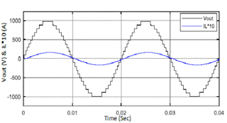
Fig. 5. Simulated performance of the system after load inclusion for sinusoidal PWM: (a) dq current components, (b) output reference signals from the controller, (c) line voltage (after filter), (d) line current (after filter), and (e) dc-link voltage.


Fig. 6. Converter output voltage profiles with momentary OVM region for different modulation schemes: (a) SPWM, (b) THSDBCPWM, (c) SSDBCPWM, and (d) THPWM.
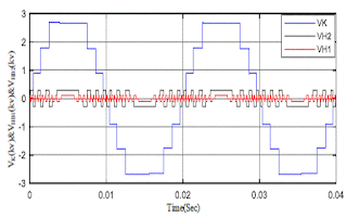

Fig. 7. (a) High-frequency gate pulses to drive high frequency inverter and (b) gate pulse generation from DSP F28335 for single phase voltage generation of five-level CHB converter (proposed OVM with third harmonic injected signal).


Fig. 8. (a) High-frequency magnetic link primary and secondary voltage with rectified output voltage and (b) primary and secondary voltage with corresponding magnetizing current.


Fig. 9. (a) B-H loop of the core with high-frequency excitation with 1.2 μs dead-band and (b) core loss with 10 kHz square wave excitation.


Fig. 10. Converter overall performance under existing (left column) and proposed (right column) OVM technique with third harmonic injected signal.
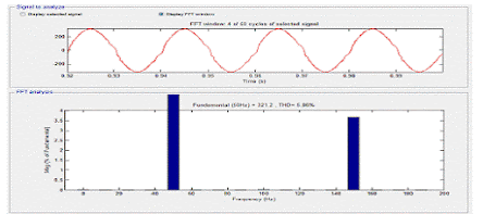
CONCLUSION:

To improve the system performance, a modified OVM technique is presented in this paper with grid connected and islanded operation. With the proposed modified carrier signal based BCPWM techniques, the overall loss and THD are decreased for both the islanded and grid connected modes compared with the traditional OVM techniques. Moreover, the voltage gain can be increased and remains approximately constant in the proposed method, which may not be possible to obtain using the traditional OVM methods. In this paper, a high-frequency magnetic link-based fully-rated CHB converter is developed for wind energy applications and the behavior of the system under rated and overrated load conditions are investigated.The use of magnetic link for the generation of isolated and balanced dc sources of the MLC inherently overcomes the voltage imbalance problem of CHB MLC and hence effectively simplifies the system control complexities. The core loss of high-frequency magnetic link is also measured to identify the overall loss of the system. The effectiveness of the proposed technology is confirmed by the simulation and experimental results.


REFERENCES:

[1] M. R. Islam, Y. G. Guo, J. G. Zhu, H. Lu, and J. X. Jin, “High-frequency magnetic-link medium-voltage converter for superconducting generator-based high-power density wind generation systems,” IEEE Trans. Appl. Supercond., vol. 24, no. 5, pp. 1–5, Oct. 2014.

[2] N. Mendis, K. M. Muttaqi, S. Perera, and S. Kamalasadan, “An effective power management strategy for a wind–diesel–hydrogen-based remote area power Supply System to meet fluctuating demands under generation uncertainty,” IEEE Trans. Ind. Appl., vol. 51, no. 2, pp. 1228–1238, Mar.–Apr. 2015.

[3] B. Jain, S. Jain, and R. K. Nema, “Control strategies of grid interfaced wind energy conversion system: An overview,” Renew. Sustain. Energy Rev., vol. 47, pp. 983–996, Apr. 2015.

[4] Y. Tan, K. M. Muttaqi, P. Ciufo, and L. Meegahapola, “Enhanced frequency response strategy for a PMSG-based wind energy conversion system using ultracapacitor in remote area power supply systems,” IEEE Trans. Ind. Appl., vol. 53, no. 1, pp. 549–558, Jan.–Feb. 2017.

[5] M. R. Islam, Y. G. Guo, and J. G. Zhu, “A multilevel medium-voltage inverter for step-up-transformer-less grid connection of photovoltaic power plants,” IEEE J. Photovolt., vol. 4, no. 3, pp. 881‒889, May 2014.