asokatechnologies@gmail.com 09347143789/09949240245

Search This Blog

Thursday, 24 February 2022

A Switched-Capacitor Inverter Using Series/Parallel Conversion With Inductive Load

 ABSTRACT:

A novel switched-capacitor inverter is proposed. The proposed inverter outputs larger voltage than the input voltage by switching the capacitors in series and in parallel. The maximum output voltage is determined by the number of the capacitors. The proposed inverter, which does not need any inductors, can be smaller than a conventional two-stage unit which consists of a boost converter and an inverter bridge. Its output harmonics are reduced compared to a conventional voltage source single phase full bridge inverter. In this paper, the circuit configuration, the theoretical operation, the simulation results with MATLAB/ SIMULINK, and the experimental results are shown. The experimental results accorded with the theoretical calculation and the simulation results.

 KEYWORDS:

1.      Charge pump

2.      Multicarrier PWM

3.      Multilevel inverter

4.      Switched capacitor (SC)

 SOFTWARE: MATLAB/SIMULINK

 CIRCUIT DIAGRAM:


Fig. 1. Circuit topology of the switched-capacitor inverter using series/ parallel conversion.

 EXPECTED SIMULATION RESULTS:


Fig. 2. Simulated voltage waveforms of the proposed inverter (n = 2) designed for low power at 5.76 [W], switching  frequency f = 40 [kHz] and reference waveform frequency fref = 1 [kHz]. (a) Bus voltage waveform vbus and (b) the output voltage waveform vout.


Fig. 3. Simulated voltage waveforms of the proposed inverter (n = 2) designed for high power at 4.50 [kW], switching frequency f = 40 [kHz] and reference waveform frequency fref = 1 [kHz]. (a) Bus voltage waveform vbus and (b) the output voltage waveform vout.


Fig. 4. Simulated current waveforms of the capacitor iC1 in the proposed inverter (n = 2).(a) Designed for low power at 5.76 [W] and (b) designed for high power at 4.50 [kW].


Fig. 5. Simulated spectra of the bus voltage waveform of the proposed inverters (n = 2) normalized with the fundamental component. (a) Designed for low power at 5.76 [W] and (b) designed for high power at 4.50 [kW].


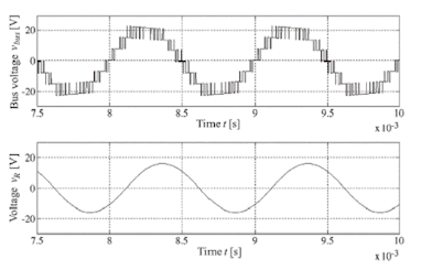
 Fig. 6. Simulated bus voltage waveforms vbus and the voltage waveforms of the load resistance vR of the proposed inverter (n = 2) designed for low power at 5.76 [W] with an inductive load.


CONCLUSION:

 In this paper, a novel boost switched-capacitor inverter was proposed. The circuit topology was introduced. The modulation method, the determination method of the capacitance, and the loss calculation of the proposed inverter were shown. The circuit operation of the proposed inverter was confirmed by the simulation results and the experimental results with a resistive load and an inductive load. The proposed inverter outputs a larger voltage than the input voltage by switching the capacitors in series and in parallel. The inverter can operate with an inductive load. The structure of the inverter is simpler than the conventional switched-capacitor inverters. THD of the output waveform of the inverter is reduced compared to the conventional single phase full bridge inverter as the conventional multilevel inverter.

REFERENCES:

[1] H. Liu, L. M. Tolbert, S. Khomfoi, B. Ozpineci, and Z. Du, “Hybrid cascaded multilevel inverter with PWM control method,” in Proc. IEEE Power Electron. Spec. Conf., Jun. 2008, pp. 162–166.

[2] A. Emadi, S. S. Williamson, and A. Khaligh, “Power electronics intensive solutions for advanced electric, hybrid electric, and fuel cell vehicular power systems,” IEEE Trans. Power Electron., vol. 21, no. 3, pp. 567–577, May 2006.

[3] L. G. Franquelo, J. Rodriguez, J. I. Leon, S. Kouro, R. Portillo, and M. A. M. Prats, “The age of multilevel converters arrives,” IEEE Ind. Electron. Mag., vol. 2, no. 2, pp. 28–39, Jun. 2008.

[4] Y. Hinago and H. Koizumi, “A single phase multilevel inverter using switched series/parallel DC voltage sources,” IEEE Trans. Ind. Electron., vol. 57, no. 8, pp. 2643–2650, Aug. 2010.

[5] S. Chandrasekaran and L. U. Gokdere, “Integrated magnetics for interleaved DC–DC boost converter for fuel cell powered vehicles,” in Proc. IEEE Power Electron. Spec. Conf., Jun. 2004, pp. 356–361.


A Quasi-Resonant Switched-Capacitor Multilevel Inverter With Self-Voltage Balancing for Single-Phase High-Frequency AC Microgrids

ABSTRACT:

 In this paper, a quasi-resonant switched-capacitor (QRSC) multilevel inverter (MLI) is proposed with self-voltage balancing for single-phase high-frequency ac (HFAC) microgrids. It is composed of a QRSC circuit (QRSCC) in the frontend and an H-bridge circuit in the backend. The input voltage is divided averagely by the series-connected capacitors in QRSCC, and any voltage level can be obtained by increasing the capacitor number. The different operational mechanism and the resulting different application make up for the deficiency of the existing switched-capacitor topologies. The capacitors are connected in parallel partially or wholly when discharging to the load, thus the self-voltage balancing is realized without any high-frequency balancing algorithm. In other words, the proposed QRSC MLI is especially adapted for HFAC fields, where fundamental frequency modulation is preferred when considering the switching frequency and the resulting loss. The quasi-resonance technique is utilized to suppress the current spikes that emerge from the instantaneous parallel connection of the series-connected capacitors and the input source, decreasing the capacitance, increasing their lifetimes, and reducing the electromagnetic interference, simultaneously. The circuit analysis, power loss analysis, and comparisons with typical switched-capacitor topologies are presented. To evaluate the superior performances, a nine-level prototype is designed and implemented in both simulation and experiment, whose results confirm the feasibility of the proposed QRSC MLI.

 KEYWORDS:

1.      High-frequency ac (HFAC) microgrids

2.      Quasi-resonant switched-capacitor (QRSC)

3.      Multilevel inverter (MLI)

4.      Self-voltage balancing

 SOFTWARE: MATLAB/SIMULINK

 CIRCUIT DIAGRAM:


Fig.1.Circuir of the proposed QRSC MLI when outputting 2n+1 levels

 EXPECTED SIMULATION RESULTS:


Fig. 2. Simulation waveforms of the output voltages and currents under different load-types. (a) Vin = 100 V, fo = 500 Hz, ZL = 24 . (b) Vin = 100 V, fo = 500 Hz, ZL = 7.4+j11.3  (|ZL| = 13.5 


Fig. 3. (a) Simulation waveforms of the voltages on capacitors C1~C4. (b) Simulation frequency spectrum of the staircase output.

Fig. 4. Simulation waveforms of the capacitors’ charging currents. (a) With quasi-resonant inductor. (b) Without quasi-resonant inductor.

CONCLUSION:


To make up for the deficiency that existing SC MLIs are inappropriate for the preferred series-connected input occasions like mode 2 in Fig. 1, a novel SC MLI is proposed in this paper with different structure and operational mechanism from the traditional ones, and to suppress the current spikes caused by the capacitors’ instant charging from the input source, a quasi-resonant inductor is embedded into the capacitors’ charging loop, reducing the EMI and longing the capacitors’ lifetimes. Meanwhile, the proposed QRSC MLI combines the advantages of the traditional SC MLI, such as self-voltage balancing under FFM and smaller voltage ripples for capacitors when used as HF power conversion, thus, especially adapted for HFAC microgrids.

The circuit configuration and the power loss analysis of the proposed QRSC MLI have been presented in this paper, as well as the comparisons with typical SC topologies. Lastly, a nine-level prototype is designed and implemented in both simulation and experiment. The results have validated the superior performances of the proposed topology.

REFERENCES:


[1] J. Drobnik, “High frequency alternating current power distribution,” Proceedings of IEEE INTELEC, pp. 292-296, 1994.

[2] S. Chakraborty, M. D. Weiss, and M. G. Simões, “Distributed intelligent energy management system for a single-phase high-frequency AC microgrid,” IEEE Trans. Ind. Electron., vol. 54, no. 1, pp. 97-109, Feb. 2007.

[3] S. Chakraborty and M. G. Simões, “Experimental evaluation of active filtering in a single-phase high-frequency AC microgrid,” IEEE Trans. Energy Convers., vol. 24, no. 3, pp. 673-682, Sept. 2009.

[4] S. B. Kjaer, J. K. Pedersen, and Frede Blaabjerg, “A review of single-phase grid-connected inverters for photovoltaic modules,” IEEE Trans. Ind. Appl., vol. 41, no. 5, pp. 1292–1306, Sep./Oct. 2005.

[5] J. Liu, K. W. E. Cheng, and J. Zeng, “A unified phase-shift modulation for optimized synchronization of parallel resonant inverters in high frequency power distribution system.” IEEE Trans. Ind. Electron., vol. 61, no. 7, pp. 3232,3247, Jul. 2014.


A PWM Strategy Based on State Transition for Cascaded H-Bridge Inverter under Unbalanced DC Sources

 ABSTRACT:

 Cascaded H-bridge converter has been widely used and researched in industry, since it is suitable for the operation under both normal and fault conditions. This paper proposes a novel PWM strategy based on state transition for cascaded H-Bridge inverter with unbalanced DC sources to achieve high quality line-to-line output voltages and maximize the linear modulation range. In this modulation strategy, the duration time of each switching state will be modified directly through the correction value. Ranges of correction value are derived by analyzing the modulation index limitation. Then, proper correction value is added into duration times to transform the switching states and extend modulation index to the maximum value. Meanwhile, balanced AC currents can be obtained under unbalanced DC sources condition, even under larger unbalanced coefficients. Furthermore, a three-phase power control algorithm (PCA) is introduced to achieve the balanced distribution of three-phase power. Compared with the traditional zero-sequence voltage injection method, the proposed strategy is more convenient and effective theoretically, and it can be applied to the higher-level cascaded H-bridge converter. The advantage and effectiveness of the proposed strategy are verified by simulation and experiment results.

KEYWORDS:

1.      State transition

2.      Linear modulation range

3.      Unbalanced DC sources

4.      Power control algorithm

SOFTWARE: MATLAB/SIMULINK

BLOCK DIAGRAM:


Fig. 1. Circuit of Cascaded H-Bridge Converter.

 EXPECTED SIMULATION RESULTS


Fig. 2. The simulation results with ten cells per phase under m =0.9 (a) line-to-line voltages uXX of simplified SVM and ST-PWM(b) output AC currents iX of simplified SVM and ST-PWM

 CONCLUSION:


A novel PWM strategy based on state transition for CHBI with unbalanced DC sources has been proposed in this paper. Compared with ZSVIM and NVM, the duration times of each switch states can be modified directly by correction value and the gate signals can be acquired easily through ST-PWM. To acquire the maximum linear modulation index, the reason of the modulation index limitation and the novel modulation strategy based on the state transition are studied. The proposed strategy can achieve high quality line-to-line output voltages and extend the modulation range as high as possible. Besides, the three-phase power control algorithm is introduced to acquire balanced power distribution. The effectiveness has been verified by simulation and experiment results.

In our current work, we incorporate PCA into the ST-PWM strategy, which is a prototype of multi-objective control. Since both modulation index extension and power control are achieved by adjusting ΔT, there is a conflict on the control objectives. That is to say, the control ability of PCA will decrease when the modulation index is extended. However, we have not yet found a strict mathematical relationship between them due to time constraints. And we will do a further research on multi-objective optimal PWM strategy and multi-objective control boundaries under unbalanced dc sources in the future.

REFERENCES:


[1] A. Marzoughi, R. Burgos, D. Boroyevich, and Y. Xue, "Investigation and comparison of cascaded H-bridge and modular multilevel converter topologies for medium-voltage drive application," in Industrial Electronics Society, IECON 2014 - 40th Annual Conference of the IEEE, 2014, pp. 1562-1568.

[2] S. Kouro, M. Malinowski, K. Gopakumar, J. Pou, L. G. Franquelo, B. Wu, et al., "Recent Advances and Industrial Applications of Multilevel Converters," IEEE Trans. Ind. Electron., vol. 57, no. 8, pp. 2553-2580, Aug. 2010.

[3] X. Zha, L. Xiong, J. Gong and F. Liu, "Cascaded multilevel converter for medium-voltage motor drive capable of regenerating with part of cells," IET Power Electronics, vol. 7, no. 5, pp. 1313-1320, May. 2014.

[4] G. Farivar, C. D. Townsend, B. Hredzak, J. Pou, and V. G. Agelidis, "Low-capacitance cascaded H-bridge multilevel StatCom," IEEE Trans. Power Electron., vol. 32, no. 3, pp. 744-1754, Mar. 2017.

[5] K. D. Teryima, G. Y. Nentawe, and A. O. David, "A Overlapping Carrier Based SPWM for a 5-Level Cascaded H-bridge Multilevel Inverter," International Journal of Power Electronics and Drive Systems (IJPEDS), vol. 7, no. 2, pp. 349-357, 2016.

A Novel Nine-Level Inverter Employing One Voltage Source and Reduced Components as High Frequency AC Power Source

 ABSTRACT:

Increasing demands for power supplies have contributed to the population of high frequency ac (HFAC) power distribution system (PDS), and in order to increase the power capacity, multilevel inverters (MLIs) frequently serving as the high-frequency (HF) source-stage have obtained a prominent development. Existing MLIs commonly use more than one voltage source or a great number of power devices to enlarge the level numbers, and HF modulation (HFM) methods are usually adopted to decrease the total harmonic distortion (THD). All of these have increased the complexity and decreased the efficiency for the conversion from dc to HF ac. In this paper, a nine-level inverter employing only one input source and fewer components is proposed for HFAC PDS. It makes full use of the conversion of series and parallel connections of one voltage source and two capacitors to realize nine output levels, thus lower THD can be obtained without HFM methods. The voltage stress on power devices is relatively relieved, which has broadened its range of applications as well. Moreover, proposed nine-level inverter is equipped with the inherent self-voltage balancing ability, thus the modulation algorithm gets simplified. The circuit structure, modulation method, capacitor calculation, loss analysis and performance comparisons are presented in this paper, and all the superior performances of proposed nine-level inverter are verified by simulation and experimental prototypes with rated output power of 200W. The accordance of theoretical analysis, simulation and experimental results confirms the feasibility of proposed nine-level inverter.


KEYWORDS:

1.      Nine-level inverter

2.      One voltage source

3.      Two capacitors

4.      Self-voltage balancing

SOFTWARE: MATLAB/SIMULINK

BLOCK DIAGRAM:


Fig. 1. Circuit of proposed nine-level inverter.

EXPECTED SIMULATION RESULTS:


Fig. 2. Simulation waveforms of driving signals.


Fig. 3. Simulation waveforms of output voltages and currents under different load-types. (a) Ro = 32 . (b) ZL = 24+j20 Ro =24 Lo = 3.2 mHL31.2= 40.


Fig. 4. Simulation waveforms of the staircase output and capacitors’ voltages.


Fig. 5. Simulation waveform of frequency spectrum at fundamental frequency of 1 kHz.


CONCLUSION:

 In this paper, a novel nine-level inverter is proposed for HFAC PDS. Compared with the existing topologies, proposed topology can achieve nine-level staircase output with only one voltage source, fewer power devices and relatively less voltage stress. All these have enlarged its application scopes. Voltage balance problem is avoided by the inherent self-voltage balancing ability, which has simplified the modulation circuits or algorithms, and the lower THD of 3.13% is realized without using HFM methods. As a result, the switching loss is significantly reduced. The capacitor calculation and power loss analysis are conducted in this paper, and the comparisons with existing topologies further testify the superiority of proposed HF inverter. All the merits and the feasibility of proposed topology are evaluated by a simulation model and an experimental prototype with rate power of 200W, and their results illustrate that proposed inverter is a preferable topology to implement HF power source for HFAC PDS.

REFERENCES:

[1] J. Drobnik, “High frequency alternating current power distribution,” Proceedings of IEEE INTELEC, pp. 292-296, 1994.

[2] P. Jain, H. Pinheiro, “Hybrid high frequency AC power distribution architecture for telecommunication systems,” IEEE Trans. Power Electron., vol. 4, no.3, Jan. 1999.

[3] B. K. Bose, M.-H. Kin and M. D. Kankam, “High frequency AC vs. DC

distribution system for next generation hybrid electric vehicle,” in Proc. IEEE Int. Conf. Ind. Electron., Control, Instrum, (IECON), Aug. 5-10, 1996, vol.2, pp. 706-712.

[4] S. Chakraborty and M. G. Simões, “Experimental Evaluation of Active Filtering in a Single-Phase High-Frequency AC Microgrid,” IEEE Trans. Energy Convers., vol. 24, no. 3, pp. 673-682, Sept. 2009.

[5] R. Strzelecki and G. Benysek, Power Electronics in Smart Electrical Energy Networks. London, U.K., Springer-Verlag, 2008.


A Novel Multilevel Multi-Output Bidirectional Active Buck PFC Rectifier

 ABSTRACT:

This paper presents a new family of buck type PFC (power factor corrector) rectifiers that operates in CCM (continuous conduction mode) and generates multilevel voltage waveform at the input. Due to CCM operation, commonly used AC side capacitive filter and DC side inductive filter are removed from the proposed modified packed U-cell rectifier structure. Dual DC output terminals are provided to have a 5-level voltage waveform at the input points of the rectifier where it is supplied by a grid via a line inductor. Producing different voltage levels reduces the voltage harmonics which affects the grid current harmonic contents directly. Low switching frequency of the proposed rectifier is a distinguished characteristic among other buck type rectifiers that reduces switching losses and any high switching frequency related issues, significantly. The proposed transformer-less, reduced filter and multilevel rectifier topology has been investigated experimentally to validate the good dynamic performance in generating and regulating dual 125V DC outputs terminals as telecommunication boards feeders or industrial battery chargers under various situation including change in the loads and change in the in main grid voltage amplitude.

KEYWORDS:

1.      Packed U-Cell

2.      PUC5

3.      HPUC

4.      Buck PFC rectifier

5.      Multilevel converter

6.      Power quality

SOFTWARE: MATLAB/SIMULINK

 BLOCK DIAGRAM:


Fig. 1. Proposed HPUC five-level buck PFC rectifier

 EXPECTED SIMULATION RESULTS:


Fig. 2. Experimental results of the proposed HPUC rectifier connected to 120V RMS AC grid and supplying two DC loads at 125V DC. a) Output DC voltages regulated at 125V with grid side synchronised voltage and current b) DC loads currents with grid side synchronised voltage and current c) 5-Level voltage waveform at the input of the HPUC rectifier d) RMS and THD values of the AC side synchronised voltage and current waveforms


Fig. 3. Test results during 200% increase in Load1 from 53_ to 160_


Fig. 4. Test results during 50% decrease in Load2 from 80_ to 40_


Fig. 5. Supply voltage variation while the output DC voltages are regulated at 125V as buck mode of operation.


CONCLUSION:


In this paper a 5-level rectifier operating in buck mode has been proposed which is called HPUC as a slight modification to PUC multilevel converter. It has been demonstrated that the proposed rectifier can deceive the grid by generating maximum voltage level of 250V at AC side as boost mode while splitting this voltage value at its two output terminals to provide buck mode of operation with 125V DC useable for battery chargers or telecommunication boards’ feeder. Although it has more active switches than other buck rectifier topologies and some limitations on power balance between loads, overall system works in boost mode and CCM which results in removing bulky AC and DC filters that usually used in conventional buck PFC rectifiers. Moreover, generating multilevel waveform leads to reduced harmonic component of the voltage waveform and consequently the line current. It also aims at operating with low switching frequency and small line inductor that all in all characterizes low power losses and high efficiency of the HPUC rectifier. Comprehensive theoretical studies and simulations have been performed on power balancing issue of the HPUC rectifier. Full experimental results in steady state and during load and supply variation have been illustrated to prove the fact that HPUC topology can be a good candidate in a new family of buck bridgeless PFC rectifiers with acceptable performance. Future works can be devoted to developing robust and nonlinear controllers on the proposed rectifier topology.

REFERENCES:

[1] M. Mobarrez, M. G. Kashani, G. Chavan, and S. Bhattacharya, "A Novel Control Approach for Protection of Multi-Terminal VSC based HVDC Transmission System against DC Faults," in ECCE 2015- Energy Conversion Congress & Exposition, Canada, 2015, pp. 4208- 4213.

[2] IEEE, "IEEE Recommended Practice and Requirements for Harmonic Control in Electric Power Systems," in IEEE Std 519-2014 (Revision of IEEE Std 519-1992), ed, 2014, pp. 1-29.

[3] IEC, "Limits for Harmonic Current Emissions (Equipment Input Current_ 16A Per Phase)," in IEC 61000-3-2 (Ed. 3.2, 2009), ed, 1995.

[4] B. Singh, B. N. Singh, A. Chandra, K. Al-Haddad, A. Pandey, and D. P. Kothari, "A review of single-phase improved power quality ACDC converters," IEEE Trans. Ind. Electron., vol. 50, no. 5, pp. 962- 981, 2003.

[5] H. Choi, "Interleaved boundary conduction mode (BCM) buck power factor correction (PFC) converter," IEEE Trans. Power Electron., vol. 28, no. 6, pp. 2629-2634, 2013.