An Integrated Boost Resonant Converter for Photovoltaic Applications
Abstract:
Effective photovoltaic power conditioning requires efficient
power conversion and accurate maximum power point tracking to counteract the
effects of panel mismatch, shading, and general variance in power output during
a daily cycle. In this paper, the authors propose an integrated boost resonant
converter with low component count, galvanic isolation, simple control, as well
as
high efficiency across a wide input and load range.
Provided is a discussion of the converter synthesis, key operational features,
converter design procedure, and loss analysis, as well as experimental verification
by way of a 250-W prototype with a California Energy Commission efficiency of
96.8%.
Keywords:
1.
Integrated
boost resonant (IBR)
2.
Isolated dc–dc
micro converter
3.
photovoltaic
(PV)
Software: MATLAB/SIMULINK
Block Diagram:
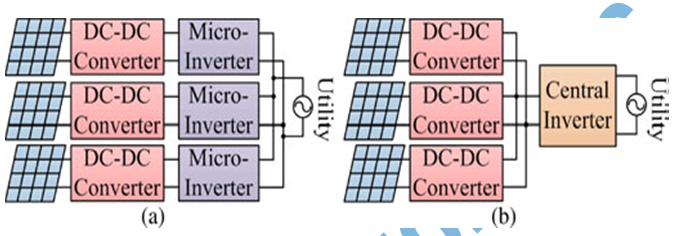
Fig. 1. Distributed
(a)microinverter and (b) microconverter system structures.
Conclusion:
As a solution for providing
efficient, distributed PV conversion, an isolated boost resonant converter has
been proposed. The system is a hybrid between a traditional CCM boost converter
and a series-resonant half-bridge, employing only two active switches. The
synthesis of the converter was described along with the circuit operating modes
and key waveforms. The design process was then defined, with a focus on the
unique combined resonant and PWM behavior. The result was a simple process,
requiring only consideration of the resonant period length in selecting a valid
converter duty cycle range. Also provided
was a detailed theoretical loss
analysis, along with formulas for calculating the rms values of important
waveforms. Finally, the loss and theoretical analysis were verified by the design,
construction, and testing of a 250-W experimental prototype. The principle
advantages of utilizing this topology were as follows:
1) high weighted efficiency because
of low circulating energy and reduced switching loss with
resonant energy transfer and output diode
ZCS;
2) low potential cost due to minimal
number of active devices and a small overall component
count;
3) galvanic isolation allows for the
use of high efficiency inverter stages without additional concern over ground leakage current;
4) reduced control complexity
provides lower auxiliary power loss and simpler controller IC configurations.
Further efficiency improvements
are possible with the addition of wide band gap semiconductor devices and
passive component optimization.
References:
[1]
A. S. Masoum, F. Padovan, and M. A. S. Masoum, “Impact of partial shading on
voltage- and current-based maximum power point tracking of solar modules,” in Proc.
IEEE PES General Meet., 2010, pp. 1–5.
[2]
B. Brooks and C. Whitaker. (2005). Guideline for the use of the Performance Test
Protocol for Evaluating Inverters Used in Grid-Connected Photovoltaic Systems [Online].
Available: http://www.gosolarcalifornia.
org/equipment/documents/Sandia_Guideline_2005.pdf
[3]
W. Bower, C. Whitaker, W. Erdman, M. Behnke, and M. Fitzgerald. (2004). Performance
Test Protocol for Evaluating Inverters Used in Grid-Connected
Photovoltaic Systems [Online]. Available:http://www.gosolarcalifornia.org/equipment/documents/2004-11-22_Test_Protocol.pdf
[4]
O. Lopez, R. Teodorescu, F. Freijedo, and J. DovalGandoy, “Leakage current
evaluation of a single-phase transformerless PVinverter connected to the grid,”
in Proc. IEEE Appl. Power Electron. Conf., 2007, pp. 907– 912.
[5]
W. Yu, J.-S. Lai, H. Qian, and C. Hutchens, “High-efficiency MOSFET inverter with
H6-type configuration for photovoltaic nonisolated ac-module applications,” IEEE
Trans. Power Electron., vol. 26, no. 4, pp. 1253–1260, Apr. 2011