ABSTRACT:
As the voltage gain of converter increases with the same ratio, the current gain also increases, this increase in current gains will affect the size of the input and the output capacitor. To reduce the ripple in the input current with simultaneous decreasing the input current ripple, a novel current fed interleaved high gain converter is proposed by utilizing the interleaved front-end structure and Cockcroft Walton (CW)-Voltage Multiplier (VM). The ``current fed'' term is used because, in proposed circuitry, all the capacitors of CW-VM are energized by a current path via inductors of the interleaved structure. The proposed converter can be applied as an input boost up the stage for low voltage battery energy storage systems, photovoltaic (PV) and fuel cell (FC) based DC-AC applications. The anticipated topology consists of the two low voltage rating switches. The main benefits of the anticipated converter configuration are the continuous (ripple free) input current, high voltage gain, reduced switch rating, high reliability, easy control structure and a high percentage of efficiency. The proposed converter's working principle, mathematical based steady state analysis, and detailed component design are discussed. The parasitic of the components has been considered in the analysis to show the deviation from the ideal cases. A detailed comparison with the other available converters is presented. The experimental results of the 300W prototype are developed to confirm the performance and functionality of the anticipated DC-DC converter.
KEYWORDS:
1. Non-isolated
2. Inverting
3. Interleaved
4. High
gain
5. Renewable
6. Current
fed
7. Voltage
multiplier
SOFTWARE: MATLAB/SIMULINK
SCHEMATIC DIAGRAM:

Figure 1. Proposed Inverting High Gain Dc-Dc Converter.
EXPECTED SIMULATION RESULTS:

Figure 2. Input And Output: Voltage And Current
Waveforms.

Figure 3. Inductor Voltages And Currents
Waveforms.

Figure4. Input And Inductor Current Waveforms.
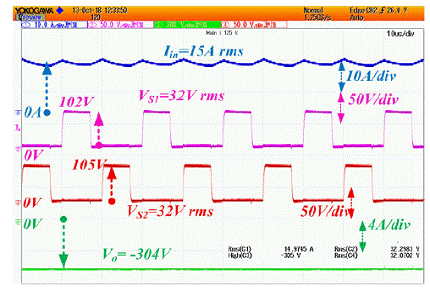
Figure 5. Switch Voltages And Input Current And
Output Voltage Waveforms.

Figure 6. Switch Voltages, Input And Inductor
Currents Waveforms.

Figure 7. Diode D1 And D2 Voltages And Inductor
Currents Waveforms.

Figure 8. Capacitor Across Capacitor C1 And C2
Waveforms.

Figure 9. Voltage Difference Between Capacitors
Waveforms.
CONCLUSION:
A
novel non-isolated current fed interleaved inverting high gain DC-DC power
converter is reported for the renewable applications. The reported converter
combines the feature of the interleaved fundamental boost converter & diode
capacitor stages. The full-wave voltage multiplier arrangement is incorporated
to raise the voltage gain by using a very minimal number of devices. At the
same duty cycle, the proposed converter be able to easily extend to the greater
numeral of stages to increase the gain by adding only 1 diode & 1 capacitor
for each VM stage increment. The detailed operating modes for CCM & DCM are
studied with the help of practical design criterion. The practical and the
theoretical voltage gains at the same duty ratios has been validated and they
are approximately equal. The detailed comparison with the recently proposed
other converter has shown that the anticipated converter is further superior
over the available converter topologies. The fabricated prototype is tested at 300W
and observed conversion is efficiency 93.07% and presented experimental results
to confirm the performance and theoretical analysis. The closed-loop control,
integration with renewable energy systems, soft switching of semiconductors devices
and voltage stress minimization of semiconductor devices are the future tasks
of the proposed converter.
REFERENCES:
[2]
Texas Instruments. TPS63700 Datasheet. (Jun. 2013). [Online]. Available:
http://www.ti.com-/lit/ds/symlink/tps-63700.pdf
[3]
S.-W. Hong, S.-H. Park, T.-H. Kong, and G.-H. Cho, ``Inverting buck-boost DC-DC
converter for mobile AMOLED display using real-time self-tuned minimum
power-loss tracking (MPLT) scheme with lossless soft-switching for
discontinuous conduction mode,'' IEEE J. Solid-State Circuits, vol. 50,
no. 10, pp. 2380_2393, Oct. 2015.
[4]
M. Jabbari, ``Resonant inverting-buck converter,'' IET Power Electron., vol.
3, no. 4, pp. 571_577, Jul. 2010.
[5]
Y. P. Siwakoti, F. Z. Peng, F. Blaabjerg, P. C. Loh, and G. E. Town, ``Impedance-source
networks for electric power conversion Part I: A topological review,'' IEEE
Trans. Power Electron., vol. 30, no. 2, pp. 699_716, Feb. 2015.
[6]
T.-J. Liang, J.-H. Lee, S.-M. Chen, J.-F. Chen, and L.-S. Yang, ``Novel isolated
high-step-up DC_DC converter with voltage lift,'' IEEE Trans. Ind. Electron.,
vol. 60, no. 4, pp. 1483_1491, Apr. 2013.